EVAL-ADUC824QS Analog Devices Inc, EVAL-ADUC824QS Datasheet - Page 28
EVAL-ADUC824QS
Manufacturer Part Number
EVAL-ADUC824QS
Description
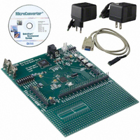
KIT DEV FOR ADUC824 QUICK START
Manufacturer
Analog Devices Inc
Series
QuickStart™ Kitr
Type
8052-corer
Datasheet
1.EVAL-ADUC824QSZ.pdf
(68 pages)
Specifications of EVAL-ADUC824QS
Contents
Evaluation Board, Power Supply, Cable, Software and Documentation
For Use With/related Products
ADuC824
Lead Free Status / RoHS Status
Contains lead / RoHS non-compliant


ADuC824
ADC1CON (Auxiliary ADC Control Register)
Used to configure the Auxiliary ADC for channel selection, external Ref enable and unipolar or bipolar coding. It should be noted that the
Auxiliary ADC only operates on a fixed input range of ± V
SFR Address
Power-On Default Value
Bit Addressable
Bit
7
6
5
4
3
2
1
0
*NOTES
1. When the temperature sensor is selected, user code must select internal reference via XREF1 bit above and clear the UNI1 bit (ADC1CON.3) to select bipolar coding.
2. The temperature sensor is factory calibrated to yield conversion results 8000H at 0 °C.
3. A +1°C change in temperature will result in a +1 LSB change in the ADC1H register ADC conversion result.
SF (Sinc Filter Register)
The number in this register sets the decimation factor and thus
the output update rate for the Primary and Auxiliary ADCs.
This SFR cannot be written by user software while either ADC is
active. The update rate applies to both Primary and Auxiliary
ADCs and is calculated as follows:
Where:
The allowable range for SF is 0Dhex to FFhex. Examples of SF
values and corresponding conversion update rate (f
—
f
f
SF =
ADC
MOD
Name
—
XREF1
ACH1
ACH0
UNI1
—
—
—
=
= Modulator Clock Frequency = 32.768 kHz
f
X
ADC
ADC Output Update Rate
Decimal Value of SF Register
R
E
=
F
1
3
1
×
8
.
SF
1
Auxiliary ADC External Reference Bit
Auxiliary ADC Channel Selection Bits
D3H
00H
No
Description
Reserved for Future Use
Set by user to enable the Auxiliary ADC to use the external reference via REFIN(+)/REFIN(–).
Cleared by user to enable the Auxiliary ADC to use the internal bandgap reference.
Written by the user to select the single-ended input pins used to drive the Auxiliary ADC as follows:
ACH1
0
0
1
1
Auxiliary ADC Unipolar Bit
Set by user to enable unipolar coding, i.e., zero input will result in 0000 hex output.
Cleared by user to enable bipolar coding, zero input will result in 8000 hex output.
Reserved for Future Use
Reserved for Future Use
Reserved for Future Use
×
A
f
C
MOD
H
1
Table VI. ADC1CON SFR Bit Designations
ACH0
0
1
0
1
ADC
) and con-
A
C
REF
H
0
.
Positive Input
AIN3
AIN4
Temp Sensor*
AIN5
–28–
version time (t
value for the SF register is 45hex, resulting in a default ADC
update rate of just under 20 Hz. Both ADC inputs are chopped
to minimize offset errors, which means that the settling time for
a single conversion or the time to a first conversion result in
continuous conversion mode is 2 × t
all calibration cycles will be carried out automatically with a
maximum, i.e., FFhex, SF value to ensure optimum calibra-
tion performance. Once a calibration cycle has completed, the
value in the SF register will be that programmed by user software.
SF(dec)
13
69
255
U
N
1 I
Negative Input
AGND
AGND
AGND (Temp. Sensor routed to the ADC input)
AGND
Table VII. SF SFR Bit Designations
ADC
) are shown in Table VII, the power-on default
SF(hex)
FF
0D
45
—
f
105.3
19.79
5.35
ADC
ADC
—
. As mentioned earlier,
(Hz)
t
9.52
50.34
186.77
ADC
—
REV. B
(ms)
Related parts for EVAL-ADUC824QS
Image
Part Number
Description
Manufacturer
Datasheet
Request
R


Part Number:
Description:
BOARD EVAL FOR SI270X-A
Manufacturer:
Silicon Laboratories Inc
Datasheet:

Part Number:
Description:
BUCK CONV REF DESIGN KIT IP1201
Manufacturer:
International Rectifier
Datasheet:
Part Number:
Description:
BOARD DEMO SYNC DUAL BUCK CNVTER
Manufacturer:
International Rectifier
Datasheet:
Part Number:
Description:
BOARD DEMO SYNC BUCK CONVETER
Manufacturer:
International Rectifier
Datasheet:

Part Number:
Description:
EVALBOARD/EB Omnidirectional microphone - Analog
Manufacturer:
Analog Devices
Datasheet:
Part Number:
Description:
EVALBOARD/EB Omnidirectional microphone - Analog
Manufacturer:
Analog Devices
Datasheet:


Part Number:
Description:
BOARD EVAL LED DRIVER LT3756
Manufacturer:
Linear Technology
Datasheet:

Part Number:
Description:
BOARD EVAL FOR AD7741/7742
Manufacturer:
Analog Devices Inc
Datasheet:

Part Number:
Description:
±1.7g Dual-Axis IMEMS Accelerometer Evaluation Board
Manufacturer:
Analog Devices Inc
Datasheet:

Part Number:
Description:
IC MULTIPLIER ANALOG 8-SOIC T/R
Manufacturer:
Analog Devices Inc
Datasheet:

Part Number:
Description:
IC ANALOG MULTIPLIER 8-DIP
Manufacturer:
Analog Devices Inc
Datasheet:
Part Number:
Description:
IC ANALOG MULTIPLIER 8-SOIC
Manufacturer:
Analog Devices Inc
Datasheet:
Part Number:
Description:
IC ANALOG MULTIPLIER 8-DIP
Manufacturer:
Analog Devices Inc
Datasheet: