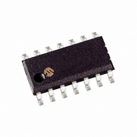
PIC16F688T-I/SL Microchip Technology, PIC16F688T-I/SL Datasheet - Page 142

PIC16F688T-I/SL
Manufacturer Part Number
PIC16F688T-I/SL
Description
IC MCU PIC FLASH 4KX14 14SOIC
Manufacturer
Microchip Technology
Series
PIC® 16Fr
Datasheets
1.PIC16F616T-ISL.pdf
(8 pages)
2.PIC16F688T-ISL.pdf
(204 pages)
3.PIC16F688T-ISL.pdf
(6 pages)
4.PIC16F688T-ISL.pdf
(4 pages)
5.PIC16F688T-ISL.pdf
(688 pages)
Specifications of PIC16F688T-I/SL
Core Size
8-Bit
Program Memory Size
7KB (4K x 14)
Core Processor
PIC
Speed
20MHz
Connectivity
UART/USART
Peripherals
Brown-out Detect/Reset, POR, WDT
Number Of I /o
12
Program Memory Type
FLASH
Eeprom Size
256 x 8
Ram Size
256 x 8
Voltage - Supply (vcc/vdd)
2 V ~ 5.5 V
Data Converters
A/D 8x10b
Oscillator Type
Internal
Operating Temperature
-40°C ~ 85°C
Package / Case
14-SOIC (3.9mm Width), 14-SOL
Controller Family/series
PIC16F
No. Of I/o's
12
Eeprom Memory Size
256Byte
Ram Memory Size
256Byte
Cpu Speed
20MHz
No. Of Timers
2
Lead Free Status / RoHS Status
Lead free / RoHS Compliant
For Use With
XLT14SO-1 - SOCKET TRANSITION 14SOIC 150/208AC162061 - HEADER INTRFC MPLAB ICD2 20PINAC162056 - HEADER INTERFACE ICD2 16F688
Lead Free Status / RoHS Status
Lead free / RoHS Compliant, Lead free / RoHS Compliant
Other names
PIC16F688T-I/SL
PIC16F688T-I/SLTR
PIC16F688T-I/SLTR
Available stocks
Company
Part Number
Manufacturer
Quantity
Price
Company:
Part Number:
PIC16F688T-I/SL
Manufacturer:
BOURNS
Quantity:
45 000
Part Number:
PIC16F688T-I/SL
Manufacturer:
MICROCHIP/微芯
Quantity:
20 000
- PIC16F616T-ISL PDF datasheet
- PIC16F688T-ISL PDF datasheet #2
- PIC16F688T-ISL PDF datasheet #3
- PIC16F688T-ISL PDF datasheet #4
- PIC16F688T-ISL PDF datasheet #5
- Current page: 142 of 688
- Download datasheet (3Mb)
PICmicro MID-RANGE MCU FAMILY
9.1
DS31009A-page 9-2
Introduction
General purpose I/O pins can be considered the simplest of peripherals. They allow the
PICmicro™ to monitor and control other devices. To add flexibility and functionality to a device,
some pins are multiplexed with an alternate function(s). These functions depend on which
peripheral features are on the device. In general, when a peripheral is functioning, that pin may
not be used as a general purpose I/O pin.
For most ports, the I/O pin’s direction (input or output) is controlled by the data direction register,
called the TRIS register. TRIS<x> controls the direction of PORT<x>. A ‘1’ in the TRIS bit corre-
sponds to that pin being an input, while a ‘0’ corresponds to that pin being an output. An easy
way to remember is that a ‘1’ looks like an I (input) and a ‘0’ looks like an O (output).
The PORT register is the latch for the data to be output. When the PORT is read, the device reads
the levels present on the I/O pins (not the latch). This means that care should be taken with
read-modify-write commands on the ports and changing the direction of a pin from an input to an
output.
Figure 9-1
be multiplexed onto the I/O pin. Reading the PORT register reads the status of the pins whereas
writing to it will write to the port latch. All write operations (such as BSF and BCF instructions) are
read-modify-write operations. Therefore a write to a port implies that the port pins are read, this
value is modified, and then written to the port data latch.
Figure 9-1: Typical I/O Port
WR PORT
WR TRIS
RD PORT
Data bus
Note: I/O pin has protection diodes to V
shows a typical I/O port. This does not take into account peripheral functions that may
Data Latch
TRIS Latch
D
CK
D
CK
RD TRIS
Q
Q
Q
Q
DD
and V
Q
SS
EN
.
D
V
V
P
N
DD
SS
1997 Microchip Technology Inc.
Trigger
Schmitt
TTL or
I/O pin
Related parts for PIC16F688T-I/SL
Image
Part Number
Description
Manufacturer
Datasheet
Request
R

Part Number:
Description:
Manufacturer:
Microchip Technology Inc.
Datasheet:

Part Number:
Description:
IC PIC MCU FLASH 4KX14 14SOIC
Manufacturer:
Microchip Technology
Datasheet:

Part Number:
Description:
IC MCU FLASH 4KX14 14TSSOP
Manufacturer:
Microchip Technology
Datasheet:

Part Number:
Description:
IC PIC MCU FLASH 4KX14 14DIP
Manufacturer:
Microchip Technology
Datasheet:

Part Number:
Description:
IC PIC MCU FLASH 4KX14 16QFN
Manufacturer:
Microchip Technology
Datasheet:

Part Number:
Description:
IC MCU PIC FLASH 4KX14 14SOIC
Manufacturer:
Microchip Technology
Datasheet:

Part Number:
Description:
IC PIC MCU FLASH 4KX14 14TSSOP
Manufacturer:
Microchip Technology
Datasheet:

Part Number:
Description:
IC MCU PIC FLASH 4KX14 14DIP
Manufacturer:
Microchip Technology
Datasheet:

Part Number:
Description:
IC PIC MCU FLASH 4KX14 16QFN
Manufacturer:
Microchip Technology
Datasheet:

Part Number:
Description:
IC PIC MCU FLASH 4KX14 14TSSOP
Manufacturer:
Microchip Technology
Datasheet:

Part Number:
Description:
IC, 8BIT MCU, PIC16F, 32MHZ, SOIC-18
Manufacturer:
Microchip Technology
Datasheet:

Part Number:
Description:
IC, 8BIT MCU, PIC16F, 32MHZ, SSOP-20
Manufacturer:
Microchip Technology
Datasheet:

Part Number:
Description:
IC, 8BIT MCU, PIC16F, 32MHZ, DIP-18
Manufacturer:
Microchip Technology
Datasheet:

Part Number:
Description:
IC, 8BIT MCU, PIC16F, 32MHZ, QFN-28
Manufacturer:
Microchip Technology
Datasheet:

Part Number:
Description:
IC, 8BIT MCU, PIC16F, 32MHZ, QFN-28
Manufacturer:
Microchip Technology
Datasheet:


