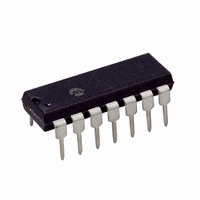
PIC16F616-I/P Microchip Technology, PIC16F616-I/P Datasheet - Page 119

PIC16F616-I/P
Manufacturer Part Number
PIC16F616-I/P
Description
IC PIC MCU FLASH 2KX14 14DIP
Manufacturer
Microchip Technology
Series
PIC® 16Fr
Datasheets
1.PIC12F609T-ISN.pdf
(26 pages)
2.PIC16F616T-ISL.pdf
(4 pages)
3.PIC16F616T-ISL.pdf
(214 pages)
4.PIC16F616T-ISL.pdf
(8 pages)
5.PIC16F616-ESL.pdf
(180 pages)
Specifications of PIC16F616-I/P
Core Size
8-Bit
Program Memory Size
3.5KB (2K x 14)
Peripherals
Brown-out Detect/Reset, POR, PWM, WDT
Core Processor
PIC
Speed
20MHz
Number Of I /o
11
Program Memory Type
FLASH
Ram Size
128 x 8
Voltage - Supply (vcc/vdd)
2 V ~ 5.5 V
Data Converters
A/D 8x10b
Oscillator Type
Internal
Operating Temperature
-40°C ~ 85°C
Package / Case
14-DIP (0.300", 7.62mm)
Controller Family/series
PIC16F
No. Of I/o's
12
Ram Memory Size
128Byte
Cpu Speed
20MHz
No. Of Timers
3
Package
14PDIP
Device Core
PIC
Family Name
PIC16
Maximum Speed
20 MHz
Operating Supply Voltage
2.5|3.3|5 V
Data Bus Width
8 Bit
Number Of Programmable I/os
11
On-chip Adc
8-chx10-bit
Number Of Timers
3
Processor Series
PIC16F
Core
PIC
Data Ram Size
128 B
Maximum Clock Frequency
20 MHz
Maximum Operating Temperature
+ 85 C
Mounting Style
Through Hole
3rd Party Development Tools
52715-96, 52716-328, 52717-734
Development Tools By Supplier
PG164130, DV164035, DV244005, DV164005, PG164120, ICE2000
Minimum Operating Temperature
- 40 C
Lead Free Status / RoHS Status
Lead free / RoHS Compliant
For Use With
MCP1631RD-DCPC1 - REF DES BATT CHARG OR LED DRIVERAC162083 - HEADER MPLAB ICD2 PIC16F616 8/14AC124001 - MODULE SKT PROMATEII 8DIP/SOIC
Eeprom Size
-
Connectivity
-
Lead Free Status / Rohs Status
Details
FIGURE 12-8:
TABLE 12-6:
© 2007 Microchip Technology Inc.
INTCON
IOCA
PIR1
PIE1
Legend:
Note
INSTRUCTION FLOW
GIE bit
(INTCON reg.)
INTF flag
(INTCON reg.)
Name
CLKOUT
INT pin
OSC1
Instruction
Executed
Note 1: INTF flag is sampled here (every Q1).
Instruction
Fetched
PC
1:
2: Asynchronous interrupt latency = 3-4 T
3: CLKOUT is available only in INTOSC and RC Oscillator modes.
4: For minimum width of INT pulse, refer to AC specifications in
5: INTF is enabled to be set any time during the Q4-Q1 cycles.
x = unknown, u = unchanged, – = unimplemented read as ‘0’, q = value depends upon condition.
Shaded cells are not used by the interrupt module.
PIC16F616/16HV616 only.
(3)
is the same whether Inst (PC) is a single cycle or a 2-cycle instruction.
Bit 7
GIE
—
—
—
SUMMARY OF REGISTERS ASSOCIATED WITH INTERRUPTS
Q1
Inst (PC – 1)
Inst (PC)
(1)
INT PIN INTERRUPT TIMING
ADIE
Q2
ADIF
PEIE
Bit 6
PC
—
(1)
(1)
Q3 Q4
(4)
CCP1IF
CCP1IE
IOCA5
(5)
Bit 5
T0IE
Q1
(1)
(1)
Inst (PC + 1)
Inst (PC)
IOCA4
Q2
(1)
INTE
Bit 4
C2IF
C2IE
PIC16F610/616/16HV610/616
PC + 1
Q3 Q4
CY
. Synchronous latency = 3 T
Preliminary
IOCA3
RAIE
Bit 3
C1IF
C1IE
Interrupt Latency
Q1
Dummy Cycle
IOCA2
Bit 2
T0IF
Q2
—
—
PC + 1
—
Q3 Q4
Section 15.0 “Electrical Specifications”
TMR2IF
TMR2IE
IOCA1
Bit 1
INTF
(2)
CY
(1)
(1)
, where T
Q1
Dummy Cycle
Inst (0004h)
TMR1IF
TMR1IE
Q2
IOCA0
Bit 0
RAIF
0004h
CY
= instruction cycle time. Latency
Q3 Q4
0000 0000
--00 0000
-000 0-00
-000 0-00
POR, BOR
Value on
Q1
DS41288C-page 117
.
Inst (0005h)
Q2
Inst (0004h)
0005h
0000 0000
--00 0000
-000 0-00
-000 0-00
Q3 Q4
Value on
all other
Resets


