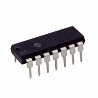
PIC16F616-I/P Microchip Technology, PIC16F616-I/P Datasheet - Page 21

PIC16F616-I/P
Manufacturer Part Number
PIC16F616-I/P
Description
IC PIC MCU FLASH 2KX14 14DIP
Manufacturer
Microchip Technology
Series
PIC® 16Fr
Datasheets
1.PIC12F609T-ISN.pdf
(26 pages)
2.PIC16F616T-ISL.pdf
(4 pages)
3.PIC16F616T-ISL.pdf
(214 pages)
4.PIC16F616T-ISL.pdf
(8 pages)
5.PIC16F616-ESL.pdf
(180 pages)
Specifications of PIC16F616-I/P
Core Size
8-Bit
Program Memory Size
3.5KB (2K x 14)
Peripherals
Brown-out Detect/Reset, POR, PWM, WDT
Core Processor
PIC
Speed
20MHz
Number Of I /o
11
Program Memory Type
FLASH
Ram Size
128 x 8
Voltage - Supply (vcc/vdd)
2 V ~ 5.5 V
Data Converters
A/D 8x10b
Oscillator Type
Internal
Operating Temperature
-40°C ~ 85°C
Package / Case
14-DIP (0.300", 7.62mm)
Controller Family/series
PIC16F
No. Of I/o's
12
Ram Memory Size
128Byte
Cpu Speed
20MHz
No. Of Timers
3
Package
14PDIP
Device Core
PIC
Family Name
PIC16
Maximum Speed
20 MHz
Operating Supply Voltage
2.5|3.3|5 V
Data Bus Width
8 Bit
Number Of Programmable I/os
11
On-chip Adc
8-chx10-bit
Number Of Timers
3
Processor Series
PIC16F
Core
PIC
Data Ram Size
128 B
Maximum Clock Frequency
20 MHz
Maximum Operating Temperature
+ 85 C
Mounting Style
Through Hole
3rd Party Development Tools
52715-96, 52716-328, 52717-734
Development Tools By Supplier
PG164130, DV164035, DV244005, DV164005, PG164120, ICE2000
Minimum Operating Temperature
- 40 C
Lead Free Status / RoHS Status
Lead free / RoHS Compliant
For Use With
MCP1631RD-DCPC1 - REF DES BATT CHARG OR LED DRIVERAC162083 - HEADER MPLAB ICD2 PIC16F616 8/14AC124001 - MODULE SKT PROMATEII 8DIP/SOIC
Eeprom Size
-
Connectivity
-
Lead Free Status / Rohs Status
Details
2.2.2.4
The PIE1 register contains the peripheral interrupt
enable bits, as shown in Register 2-4.
REGISTER 2-4:
© 2007 Microchip Technology Inc.
bit 7
Legend:
R = Readable bit
-n = Value at POR
bit 7
bit 6
bit 5
bit 4
bit 3
bit 2
bit 1
bit 0
Note 1:
U-0
—
PIC16F616/16HV616 only. PIC16F610/16HV610 unimplemented, read as ‘0’.
PIE1 Register
Unimplemented: Read as ‘0’
ADIE: A/D Converter (ADC) Interrupt Enable bit
1 = Enables the ADC interrupt
0 = Disables the ADC interrupt
CCP1IE: CCP1 Interrupt Enable bit
1 = Enables the CCP1 interrupt
0 = Disables the CCP1 interrupt
C2IE: Comparator C2 Interrupt Enable bit
1 = Enables the Comparator C2 interrupt
0 = Disables the Comparator C2 interrupt
C1IE: Comparator C1 Interrupt Enable bit
1 = Enables the Comparator C1 interrupt
0 = Disables the Comparator C1 interrupt
Unimplemented: Read as ‘0’
TMR2IE: Timer2 to PR2 Match Interrupt Enable bit
1 = Enables the Timer2 to PR2 match interrupt
0 = Disables the Timer2 to PR2 match interrupt
TMR1IE: Timer1 Overflow Interrupt Enable bit
1 = Enables the Timer1 overflow interrupt
0 = Disables the Timer1 overflow interrupt
ADIE
R/W-0
PIE1: PERIPHERAL INTERRUPT ENABLE REGISTER 1
(1)
W = Writable bit
‘1’ = Bit is set
CCP1IE
R/W-0
(1)
PIC16F610/616/16HV610/616
R/W-0
C2IE
Preliminary
(1)
U = Unimplemented bit, read as ‘0’
‘0’ = Bit is cleared
R/W-0
C1IE
(1)
Note:
(1)
Bit PEIE of the INTCON register must be
set to enable any peripheral interrupt.
U-0
—
x = Bit is unknown
TMR2IE
R/W-0
(1)
DS41288C-page 19
TMR1IE
R/W-0
bit 0


