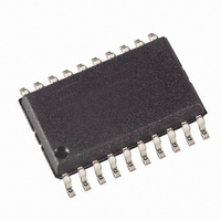
AT89LP4052-20SU Atmel, AT89LP4052-20SU Datasheet - Page 10

AT89LP4052-20SU
Manufacturer Part Number
AT89LP4052-20SU
Description
IC 8051 MCU FLASH 4K 20SOIC
Manufacturer
Atmel
Series
89LPr
Datasheet
1.AT89LP2052-20PU.pdf
(94 pages)
Specifications of AT89LP4052-20SU
Core Processor
8051
Core Size
8-Bit
Speed
20MHz
Connectivity
SPI, UART/USART
Peripherals
Brown-out Detect/Reset, POR, PWM, WDT
Number Of I /o
15
Program Memory Size
4KB (4K x 8)
Program Memory Type
FLASH
Ram Size
256 x 8
Voltage - Supply (vcc/vdd)
2.4 V ~ 5.5 V
Oscillator Type
Internal
Operating Temperature
-40°C ~ 85°C
Package / Case
20-SOIC (7.5mm Width)
Processor Series
AT89x
Core
8051
Data Bus Width
8 bit
Data Ram Size
256 B
Interface Type
SPI/UART
Maximum Clock Frequency
20 MHz
Number Of Programmable I/os
15
Number Of Timers
2
Operating Supply Voltage
2.4 V to 5.5 V
Maximum Operating Temperature
+ 85 C
Mounting Style
SMD/SMT
3rd Party Development Tools
PK51, CA51, A51, ULINK2
Development Tools By Supplier
AT89ISP
Minimum Operating Temperature
- 40 C
Package
20SOIC W
Device Core
8051
Family Name
AT89
Maximum Speed
20 MHz
Lead Free Status / RoHS Status
Lead free / RoHS Compliant
Eeprom Size
-
Data Converters
-
Lead Free Status / Rohs Status
Lead free / RoHS Compliant
Available stocks
Company
Part Number
Manufacturer
Quantity
Price
Company:
Part Number:
AT89LP4052-20SU
Manufacturer:
ATMEL
Quantity:
3 100
9. Restrictions on Certain Instructions
9.1
9.2
10. System Clock
10.1
10.2
10.3
10
Branching Instructions
MOVX-related Instructions, Data Memory
Crystal Oscillator
External Clock Source
System Clock Out
AT89LP2052/LP4052
The AT89LP2052/LP4052 is an economical and cost-effective member of Atmel's growing fam-
ily of microcontrollers. It contains 2/4K bytes of Flash program memory. It is fully compatible with
the MCS-51 architecture, and can be programmed using the MCS-51 instruction set. However,
there are a few considerations one must keep in mind when utilizing certain instructions to pro-
gram this device. All the instructions related to jumping or branching should be restricted such
that the destination address falls within the physical program memory space of the device, which
is 2K bytes for the AT89LP2052 and 4K bytes for the AT89LP4052. This should be the responsi-
bility of the software programmer. For example, LJMP 7E0H would be a valid instruction for the
AT89LP2052 (with 2K bytes of memory), whereas LJMP 900H would not.
The LCALL, LJMP, ACALL, AJMP, SJMP, and JMP @A+DPTR unconditional branching instruc-
tions will execute correctly as long as the programmer keeps in mind that the destination
branching address must fall within the physical boundaries of the program memory size (loca-
tions 000H to 7FFH for the AT89LP2052, 000H to FFFH for the AT89LP4052). Violating the
physical space limits may cause unknown program behavior. With the CJNE [...], DJNZ [...], JB,
JNB, JC, JNC, JBC, JZ, and JNZ conditional branching instructions, the same previous rule
applies. Again, violating the memory boundaries may cause erratic execution. For applications
involving interrupts, the normal interrupt service routine address locations of the 8051 family
architecture have been preserved.
External DATA memory access is not supported in this device, nor is external PROGRAM mem-
ory execution. Therefore, no MOVX [...] instructions should be included in the program. A typical
8051 assembler will still assemble instructions, even if they are written in violation of the restric-
tions mentioned above. It is the responsibility of the user to know the physical features and
limitations of the device being used and to adjust the instructions used accordingly.
The system clock is generated directly from one of two selectable clock sources. The two
sources are the on-chip crystal oscillator and external clock source. No internal clock division is
used to generate the CPU clock from the system clock.
When enabled, the internal inverting oscillator amplifier is connected between XTAL1 and
XTAL2 for connection to an external quartz crystal or ceramic resonator. When using the crystal
oscillator, XTAL2 should not be used to drive a board-level clock.
The external clock option is selected by setting the Oscillator Bypass fuse. This disables the
amplifier and allows XTAL1 to be driven directly by the clock source. XTAL2 may be left
unconnected.
When the System Clock Out fuse is enabled, P3.7 will output the system clock with no division
using the push-pull output mode. During Power-down the system clock will output as “1”.
3547J–MICRO–10/09


