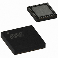
ATTINY261-20MU Atmel, ATTINY261-20MU Datasheet - Page 162

ATTINY261-20MU
Manufacturer Part Number
ATTINY261-20MU
Description
IC MCU AVR 2K FLASH 20MHZ 32-QFN
Manufacturer
Atmel
Series
AVR® ATtinyr
Specifications of ATTINY261-20MU
Core Processor
AVR
Core Size
8-Bit
Speed
20MHz
Connectivity
USI
Peripherals
Brown-out Detect/Reset, POR, PWM, WDT
Number Of I /o
16
Program Memory Size
2KB (1K x 16)
Program Memory Type
FLASH
Eeprom Size
128 x 8
Ram Size
128 x 8
Voltage - Supply (vcc/vdd)
2.7 V ~ 5.5 V
Data Converters
A/D 11x10b
Oscillator Type
Internal
Operating Temperature
-40°C ~ 85°C
Package / Case
32-VQFN Exposed Pad, 32-HVQFN, 32-SQFN, 32-DHVQFN
Processor Series
ATTINY2x
Core
AVR8
Data Bus Width
8 bit
Data Ram Size
128 B
Interface Type
2-Wire, SPI, USI
Maximum Clock Frequency
20 MHz
Number Of Programmable I/os
16
Number Of Timers
2
Maximum Operating Temperature
+ 85 C
Mounting Style
SMD/SMT
3rd Party Development Tools
EWAVR, EWAVR-BL
Development Tools By Supplier
ATAVRDRAGON, ATSTK500, ATSTK600, ATAVRISP2, ATAVRONEKIT
Minimum Operating Temperature
- 40 C
On-chip Adc
10 bit, 11 Channel
Package
32MLF EP
Device Core
AVR
Family Name
ATtiny
Maximum Speed
20 MHz
Operating Supply Voltage
3.3|5 V
For Use With
ATSTK600 - DEV KIT FOR AVR/AVR32ATAVRBC100 - REF DESIGN KIT BATTERY CHARGER770-1007 - ISP 4PORT ATMEL AVR MCU SPI/JTAGATSTK505 - ADAPTER KIT FOR 14PIN AVR MCU
Lead Free Status / RoHS Status
Lead free / RoHS Compliant
Available stocks
Company
Part Number
Manufacturer
Quantity
Price
Part Number:
ATTINY261-20MU
Manufacturer:
AVNET
Quantity:
20 000
- Current page: 162 of 242
- Download datasheet (5Mb)
15.13.5
15.13.6
162
ATtiny261/461/861
DIDR0 – Digital Input Disable Register 0
DIDR1 – Digital Input Disable Register 1
Table 15-6.
• Bits 7:4,2:0 – ADC6D:ADC0D: ADC6:0 Digital Input Disable
When this bit is written logic one, the digital input buffer on the corresponding ADC pin is dis-
abled. The corresponding PIN register bit will always read as zero when this bit is set. When an
analog signal is applied to the ADC7:0 pin and the digital input from this pin is not needed, this
bit should be written logic one to reduce power consumption in the digital input buffer.
• Bit 3 – AREFD: AREF Digital Input Disable
When this bit is written logic one, the digital input buffer on the AREF pin is disabled. The corre-
sponding PIN register bit will always read as zero when this bit is set. When an analog signal is
applied to the AREF pin and the digital input from this pin is not needed, this bit should be written
logic one to reduce power consumption in the digital input buffer.
• Bits 7:4 – ADC10D:ADC7D: ADC10:7 Digital Input Disable
When this bit is written logic one, the digital input buffer on the corresponding ADC pin is dis-
abled. The corresponding PIN register bit will always read as zero when this bit is set. When an
analog signal is applied to the ADC10:7 pin and the digital input from this pin is not needed, this
bit should be written logic one to reduce power consumption in the digital input buffer.
Bit
0x01 (0x21)
Read/Write
Initial Value
Bit
0x02 (0x22)
Read/Write
Initial Value
ADTS2
1
1
1
ADC Auto Trigger Source Selections
7
ADC6D
R/W
0
ADC10D
R/W
7
0
6
ADC5D
R/W
0
ADC9D
ADTS1
R/W
6
0
0
1
1
5
ADC4D
R/W
0
ADC8D
R/W
5
0
4
ADC3D
R/W
0
ADC7D
R/W
ADTS0
4
0
1
0
1
3
AREFD
R/W
0
R
3
0
-
Trigger Source
Timer/Counter0 Compare Match B
Timer/Counter1 Overflow
Watchdog Interrupt Request
2
ADC2D
R/W
0
R
2
0
1
ADC1D
R/W
0
R
1
0
0
ADC0D
0
R/W
R
0
0
2588E–AVR–08/10
DIDR0
DIDR1
Related parts for ATTINY261-20MU
Image
Part Number
Description
Manufacturer
Datasheet
Request
R

Part Number:
Description:
Manufacturer:
Atmel Corporation
Datasheet:

Part Number:
Description:
Manufacturer:
Atmel Corporation
Datasheet:

Part Number:
Description:
IC MCU AVR 2K FLASH 20MHZ 20-DIP
Manufacturer:
Atmel
Datasheet:

Part Number:
Description:
MCU AVR 2K FLASH 15MHZ 32-QFN
Manufacturer:
Atmel
Datasheet:

Part Number:
Description:
MCU AVR 2KB FLASH 15MHZ 32-VQFN
Manufacturer:
Atmel
Datasheet:

Part Number:
Description:
IC MCU AVR 2K FLASH 20MHZ 20SOIC
Manufacturer:
Atmel
Datasheet:

Part Number:
Description:
Attiny261 8-bit Microcontroller With 2/4/8k Bytes In-system Programmable Flash
Manufacturer:
ATMEL Corporation
Datasheet:

Part Number:
Description:
IC MCU AVR 2K FLASH 20MHZ 20SOIC
Manufacturer:
Atmel
Datasheet:

Part Number:
Description:
IC MCU AVR 2K FLASH 20MHZ 32QFN
Manufacturer:
Atmel
Datasheet:

Part Number:
Description:
Manufacturer:
Atmel Corporation
Datasheet:


