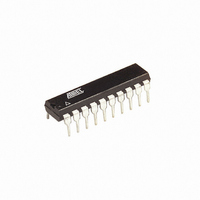
ATTINY261-20PU Atmel, ATTINY261-20PU Datasheet - Page 161

ATTINY261-20PU
Manufacturer Part Number
ATTINY261-20PU
Description
IC MCU AVR 2K FLASH 20MHZ 20-DIP
Manufacturer
Atmel
Series
AVR® ATtinyr
Specifications of ATTINY261-20PU
Core Processor
AVR
Core Size
8-Bit
Speed
20MHz
Connectivity
USI
Peripherals
Brown-out Detect/Reset, POR, PWM, WDT
Number Of I /o
16
Program Memory Size
2KB (1K x 16)
Program Memory Type
FLASH
Eeprom Size
128 x 8
Ram Size
128 x 8
Voltage - Supply (vcc/vdd)
2.7 V ~ 5.5 V
Data Converters
A/D 11x10b
Oscillator Type
Internal
Operating Temperature
-40°C ~ 85°C
Package / Case
20-DIP (0.300", 7.62mm)
Processor Series
ATTINY2x
Core
AVR8
Data Bus Width
8 bit
Data Ram Size
128 B
Interface Type
2-Wire/SPI/USI
Maximum Clock Frequency
20 MHz
Number Of Programmable I/os
16
Number Of Timers
2
Operating Supply Voltage
2.7 V to 5.5 V
Maximum Operating Temperature
+ 85 C
Mounting Style
Through Hole
3rd Party Development Tools
EWAVR, EWAVR-BL
Development Tools By Supplier
ATAVRDRAGON, ATSTK500, ATSTK600, ATAVRISP2, ATAVRONEKIT
Minimum Operating Temperature
- 40 C
On-chip Adc
11-ch x 10-bit
Data Rom Size
128 B
Height
4.95 mm
Length
26.92 mm
Supply Voltage (max)
5.5 V
Supply Voltage (min)
2.7 V
Width
7.11 mm
For Use With
ATSTK600 - DEV KIT FOR AVR/AVR32ATAVRBC100 - REF DESIGN KIT BATTERY CHARGER770-1007 - ISP 4PORT ATMEL AVR MCU SPI/JTAGATSTK505 - ADAPTER KIT FOR 14PIN AVR MCU
Lead Free Status / RoHS Status
Lead free / RoHS Compliant
Available stocks
Company
Part Number
Manufacturer
Quantity
Price
Company:
Part Number:
ATTINY261-20PU
Manufacturer:
ATMEL
Quantity:
256
- Current page: 161 of 242
- Download datasheet (5Mb)
15.13.4
2588E–AVR–08/10
ADCSRB – ADC Control and Status Register B
• Bit 7 – BIN: Bipolar Input Mode
The gain stage is working in the unipolar mode as default, but the bipolar mode can be selected
by writing the BIN bit in the ADCSRB register. In the unipolar mode only one-sided conversions
are supported and the voltage on the positive input must always be larger than the voltage on
the negative input. Otherwise the result is saturated to the voltage reference. In the bipolar mode
two-sided conversions are supported and the result is represented in the two’s complement
form. In the unipolar mode the resolution is 10 bits and the bipolar mode the resolution is 9 bits +
1 sign bit.
• Bit 6 – GSEL: Gain Select
The Gain Select bit selects the 32x gain instead of the 20x gain and the 8x gain instead of the 1x
gain when the Gain Select bit is written to one.
• Bit 5 – Res: Reserved Bit
This bit is a reserv ed bit in the ATtiny261/461/861 and will always read as zero.
• Bit 4 – REFS2: Reference Selection Bit
These bit selects either the voltage reference of 1.1 V or 2.56 V for the ADC, as shown in
15-3. If active channels are used, using AVCC or an external AREF higher than (AVCC - 1V) is
not recommended, as this will affect ADC accuracy. The internal voltage reference options may
not be used if an external voltage is being applied to the AREF pin.
• Bit 3 – MUX5: Analog Channel and Gain Selection Bit 5
The MUX5 bit is the MSB of the Analog Channel and Gain Selection bits. Refer to
details. If this bit is changed during a conversion, the change will not go into effect until this
conversion is complete (ADIF in ADCSRA is set).
• Bits 2:0 – ADTS2:0: ADC Auto Trigger Source
If ADATE in ADCSRA is written to one, the value of these bits selects which source will trigger
an ADC conversion. If ADATE is cleared, the ADTS2:0 settings will have no effect. A conversion
will be triggered by the rising edge of the selected Interrupt Flag. Note that switching from a trig-
ger source that is cleared to a trigger source that is set, will generate a positive edge on the
trigger signal. If ADEN in ADCSRA is set, this will start a conversion. Switching to Free Running
mode (ADTS[2:0]=0) will not cause a trigger event, even if the ADC Interrupt Flag is set
Table 15-6.
Bit
0x03 (0x23)
Read/Write
Initial Value
ADTS2
0
0
0
0
1
ADC Auto Trigger Source Selections
R/W
BIN
7
0
ADTS1
GSEL
R/W
6
0
0
0
1
1
0
R
5
0
-
REFS2
R/W
ADTS0
4
0
0
1
0
1
0
MUX5
R/W
3
0
Trigger Source
Free Running mode
Analog Comparator
External Interrupt Request 0
Timer/Counter0 Compare Match A
Timer/Counter0 Overflow
ADTS2
R/W
2
0
ADTS1
R/W
1
0
ADTS0
R/W
0
0
Table 15-4
ADCSRB
.
Table
161
for
Related parts for ATTINY261-20PU
Image
Part Number
Description
Manufacturer
Datasheet
Request
R

Part Number:
Description:
Manufacturer:
Atmel Corporation
Datasheet:

Part Number:
Description:
Manufacturer:
Atmel Corporation
Datasheet:

Part Number:
Description:
IC MCU AVR 2K FLASH 20MHZ 32-QFN
Manufacturer:
Atmel
Datasheet:

Part Number:
Description:
MCU AVR 2K FLASH 15MHZ 32-QFN
Manufacturer:
Atmel
Datasheet:

Part Number:
Description:
MCU AVR 2KB FLASH 15MHZ 32-VQFN
Manufacturer:
Atmel
Datasheet:

Part Number:
Description:
IC MCU AVR 2K FLASH 20MHZ 20SOIC
Manufacturer:
Atmel
Datasheet:

Part Number:
Description:
Attiny261 8-bit Microcontroller With 2/4/8k Bytes In-system Programmable Flash
Manufacturer:
ATMEL Corporation
Datasheet:

Part Number:
Description:
IC MCU AVR 2K FLASH 20MHZ 20SOIC
Manufacturer:
Atmel
Datasheet:

Part Number:
Description:
IC MCU AVR 2K FLASH 20MHZ 32QFN
Manufacturer:
Atmel
Datasheet:

Part Number:
Description:
Manufacturer:
Atmel Corporation
Datasheet:


