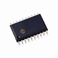
PIC18LF14K50-I/SO Microchip Technology, PIC18LF14K50-I/SO Datasheet - Page 112

PIC18LF14K50-I/SO
Manufacturer Part Number
PIC18LF14K50-I/SO
Description
IC PIC MCU FLASH 16KB 20-SOIC
Manufacturer
Microchip Technology
Series
PIC® XLP™ 18Fr
Datasheets
1.PIC18F13K50-ISS.pdf
(420 pages)
2.PIC18F13K50-ISS.pdf
(40 pages)
3.PIC18F13K50-ISS.pdf
(10 pages)
4.PIC18F13K50-ISS.pdf
(2 pages)
5.PIC18F13K50-ISO.pdf
(414 pages)
Specifications of PIC18LF14K50-I/SO
Core Size
8-Bit
Program Memory Size
16KB (8K x 16)
Core Processor
PIC
Speed
48MHz
Connectivity
I²C, SPI, UART/USART, USB
Peripherals
Brown-out Detect/Reset, POR, PWM, WDT
Number Of I /o
14
Program Memory Type
FLASH
Eeprom Size
256 x 8
Ram Size
768 x 8
Voltage - Supply (vcc/vdd)
1.8 V ~ 3.6 V
Data Converters
A/D 11x10b
Oscillator Type
Internal
Operating Temperature
-40°C ~ 85°C
Package / Case
20-SOIC (7.5mm Width)
Controller Family/series
PIC18
No. Of I/o's
15
Eeprom Memory Size
256Byte
Ram Memory Size
768Byte
Cpu Speed
48MHz
No. Of Timers
4
Processor Series
PIC18LF
Core
PIC
Data Bus Width
8 bit
Data Ram Size
256 B
Interface Type
EUSART, I2C, MSSP, SPI, USB
Maximum Clock Frequency
32 KHz
Number Of Programmable I/os
18
Number Of Timers
4
Operating Supply Voltage
1.8 V to 3.6 V
Maximum Operating Temperature
+ 125 C
Mounting Style
SMD/SMT
3rd Party Development Tools
52715-96, 52716-328, 52717-734, 52712-325, EWPIC18
Development Tools By Supplier
PG164130, DV164035, DV244005, DV164005, DM164127, DV164126
Minimum Operating Temperature
- 40 C
On-chip Adc
10 bit, 12 Channel
Lead Free Status / RoHS Status
Lead free / RoHS Compliant
Lead Free Status / RoHS Status
Lead free / RoHS Compliant, Lead free / RoHS Compliant
Available stocks
Company
Part Number
Manufacturer
Quantity
Price
Company:
Part Number:
PIC18LF14K50-I/SO
Manufacturer:
MICROCHIP
Quantity:
1 001
- PIC18F13K50-ISS PDF datasheet
- PIC18F13K50-ISS PDF datasheet #2
- PIC18F13K50-ISS PDF datasheet #3
- PIC18F13K50-ISS PDF datasheet #4
- PIC18F13K50-ISO PDF datasheet #5
- Current page: 112 of 420
- Download datasheet (4Mb)
PIC18F/LF1XK50
12.2
Timer2 can also generate an optional device interrupt.
The Timer2 output signal (TMR2-to-PR2 match) pro-
vides the input for the 4-bit output counter/postscaler.
This counter generates the TMR2 match interrupt flag
which is latched in TMR2IF of the PIR1 register. The
interrupt is enabled by setting the TMR2 Match Inter-
rupt Enable bit, TMR2IE of the PIE1 register.
A range of 16 postscale options (from 1:1 through 1:16
inclusive) can be selected with the postscaler control
bits, T2OUTPS<3:0> of the T2CON register.
FIGURE 12-1:
TABLE 12-1:
DS41350E-page 112
INTCON GIE/GIEH PEIE/GIEL
PIR1
PIE1
IPR1
TMR2
T2CON
PR2
Legend: — = unimplemented, read as ‘0’. Shaded cells are not used by the Timer2 module.
Name
T2OUTPS<3:0>
T2CKPS<1:0>
F
OSC
Timer2 Interrupt
/4
Timer2 Register
Timer2 Period Register
Bit 7
—
—
—
—
REGISTERS ASSOCIATED WITH TIMER2 AS A TIMER/COUNTER
TIMER2 BLOCK DIAGRAM
T2OUTPS3 T2OUTPS2 T2OUTPS1 T2OUTPS0 TMR2ON T2CKPS1 T2CKPS0
Internal Data Bus
1:1, 1:4, 1:16
ADIE
ADIP
ADIF
Bit 6
2
Prescaler
TMR0IE
RCIF
RCIE
RCIP
Bit 5
4
TMR2
INT0IE
TXIE
TXIP
Bit 4
TXIF
Preliminary
Reset
8
RABIE
SSPIE
SSPIP
SSPIF
Bit 3
12.3
The unscaled output of TMR2 is available primarily to
the CCP modules, where it is used as a time base for
operations in PWM mode.
Timer2 can be optionally used as the shift clock source
for the MSSP module operating in SPI mode. Addi-
tional information is provided in Section 14.0 “Master
Synchronous Serial Port (MSSP) Module”.
Comparator
1:1 to 1:16
Postscaler
8
TMR2/PR2
Match
Timer2 Output
TMR0IF
CCP1IF
CCP1IE
CCP1IP
Bit 2
TMR2IF
TMR2IE
TMR2IP
INT0IF
2010 Microchip Technology Inc.
Bit 1
PR2
8
Set TMR2IF
TMR2 Output
(to PWM or MSSP)
TMR1IF
TMR1IE
TMR1IP
RABIF
Bit 0
on page
Values
Reset
285
288
288
288
286
286
286
Related parts for PIC18LF14K50-I/SO
Image
Part Number
Description
Manufacturer
Datasheet
Request
R

Part Number:
Description:
Manufacturer:
Microchip Technology Inc.
Datasheet:

Part Number:
Description:
Manufacturer:
Microchip Technology Inc.
Datasheet:

Part Number:
Description:
Manufacturer:
Microchip Technology Inc.
Datasheet:

Part Number:
Description:
Manufacturer:
Microchip Technology Inc.
Datasheet:

Part Number:
Description:
Manufacturer:
Microchip Technology Inc.
Datasheet:

Part Number:
Description:
Manufacturer:
Microchip Technology Inc.
Datasheet:

Part Number:
Description:
Manufacturer:
Microchip Technology Inc.
Datasheet:

Part Number:
Description:
Manufacturer:
Microchip Technology Inc.
Datasheet:


