AT89C5122D-RDRUM Atmel, AT89C5122D-RDRUM Datasheet - Page 145
AT89C5122D-RDRUM
Manufacturer Part Number
AT89C5122D-RDRUM
Description
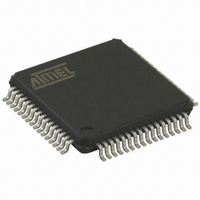
IC 8051 MCU 32K CRAM USB 64-VQFP
Manufacturer
Atmel
Series
89Cr
Datasheet
1.AT89C5122D-PSTUM.pdf
(208 pages)
Specifications of AT89C5122D-RDRUM
Core Processor
8051
Core Size
8-Bit
Speed
48MHz
Connectivity
SmartCard, SPI, UART/USART, USB
Peripherals
LED, POR, WDT
Number Of I /o
46
Program Memory Size
32KB (32K x 8)
Program Memory Type
FLASH
Ram Size
768 x 8
Voltage - Supply (vcc/vdd)
3 V ~ 5.5 V
Oscillator Type
Internal
Operating Temperature
-40°C ~ 85°C
Package / Case
64-TQFP, 64-VQFP
For Use With
AT89OCD-01 - USB EMULATOR FOR AT8XC51 MCUAT89STK-10 - KIT EVAL APPL MASS STORAGEAT89STK-03 - KIT STARTER FOR MCU AT8XC5122/23
Lead Free Status / RoHS Status
Lead free / RoHS Compliant
Eeprom Size
-
Data Converters
-
Other names
AT89C5122D-RDRUMTR
Available stocks
Company
Part Number
Manufacturer
Quantity
Price


Timers/Counters
Timer/Counter
Operations
Timer 0
4202F–SCR–07/2008
The AT8xC5122D implements two general-purpose, 16-bit Timers/Counters. Although
they are identified as Timer 0, Timer 1, you can independently configure each to operate
in a variety of modes as a Timer or as an event Counter. When operating as a Timer, a
Timer/Counter runs for a programmed length of time, then issues an interrupt request.
When operating as a Counter, a Timer/Counter counts negative transitions on an exter-
nal pin. After a preset number of counts, the Counter issues an interrupt request.
The Timer registers and associated control registers are implemented as addressable
Special Function Registers (SFRs). Two of the SFRs provide programmable control of
the Timers as follows:
•
The various operating modes of each Timer/Counter are described below.
For example, a basic operation is Timer registers THx and TLx (x= 0, 1) connected in
cascade to form a 16-bit Timer. Setting the run control bit (TRx) in the TCON register
(see Table 88 on page 150) turns the Timer on by allowing the selected input to incre-
ment TLx. When TLx overflows, it increments THx and when THx overflows it sets the
Timer overflow flag (TFx) in the TCON register. Setting the TRx does not clear the THx
and TLx Timer registers. Timer registers can be accessed to obtain the current count or
to enter preset values. They can be read at any time but the TRx bit must be cleared to
preset their values, otherwise the behavior of the Timer/Counter is unpredictable.
The C/Tx# control bit selects Timer operation or Counter operation by selecting the
divided-down system clock or the external pin Tx as the source for the counted signal.
The TRx bit must be cleared when changing the operating mode, otherwise the behavior
of the Timer/Counter is unpredictable.
For Timer operation (C/Tx#= 0), the Timer register counts the divided-down system
clock. The Timer register is incremented once every peripheral cycle.
Exceptions are the Timer 2 Baud Rate and Clock-
is incremented by the system clock divided by two.
For Counter operation (C/Tx#= 1), the Timer register counts the negative transitions on
the Tx external input pin. The external input is sampled during every S5P2 state. The
Programmer’s Guide describes the notation for the states in a peripheral cycle. When
the sample is high in one cycle and low in the next one, the Counter is incremented. The
new count value appears in the register during the next S3P1 state after the transition
has been detected. Since it takes 12 states (24 oscillator periods) to recognize a nega-
tive transition, the maximum count rate is 1/24 of the oscillator frequency. There are no
restrictions on the duty cycle of the external input signal, but to ensure that a given level
is sampled at least once before it changes, it should be held for at least one full periph-
eral cycle.
Timer 0 functions as either a Timer or an event Counter in four operating modes.
Figure 89 through Figure 95 show the logic configuration of each mode.
Timer 0 is controlled by the four lower bits of the TMOD register (see Table 89 on page
151) and bits 0, 1, 4 and 5 of the TCON register (see Table 88 on page 150). The TMOD
register selects the method of Timer gating (GATE0), Timer or Counter operation
(T/C0#) and the operating mode (M10 and M00). The TCON register provides Timer 0
control functions: overflow flag (TF0), run control bit (TR0), interrupt flag (IE0) and inter-
rupt type control bit (IT0).
Timer/Counter mode control register (TMOD) and Timer/Counter control register
(TCON) control respectively Timer 0 and Timer 1.
AT83R5122, AT8xC5122/23
O
ut modes in which the Timer register
145
Related parts for AT89C5122D-RDRUM
Image
Part Number
Description
Manufacturer
Datasheet
Request
R


Part Number:
Description:
IC 8051 MCU W/SMART CARD 64VQFP
Manufacturer:
Atmel
Datasheet:

Part Number:
Description:
IC 8051 MCU FLASH 32K 64QFN
Manufacturer:
Atmel
Datasheet:
Part Number:
Description:
IC 8051 MCU FLASH 32K 64VQFP
Manufacturer:
Atmel
Datasheet:
Part Number:
Description:
IC MCU 80C51 W/SMART CARD 64VQFP
Manufacturer:
Atmel
Datasheet:

Part Number:
Description:
IC 8051 MCU FLASH 32K 28PLCC
Manufacturer:
Atmel
Datasheet:


Part Number:
Description:
MICROCONTROLLER WITH USB AND SMART CARD READER INTERFACES
Manufacturer:
ATMEL [ATMEL Corporation]
Datasheet:

Part Number:
Description:
KIT STARTER FOR MCU AT8XC5122/23
Manufacturer:
Atmel
Datasheet:

Part Number:
Description:
IC MICRO CTRL 24MHZ 44TQFP
Manufacturer:
Atmel
Datasheet:

Part Number:
Description:
IC MICRO CTRL 24MHZ 44PLCC
Manufacturer:
Atmel
Datasheet:
Part Number:
Description:
IC MICRO CTRL 24MHZ 44PLCC
Manufacturer:
Atmel
Datasheet:

Part Number:
Description:
IC MICRO CTRL 24MHZ 40DIP
Manufacturer:
Atmel
Datasheet: