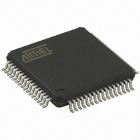
AT89C5122D-RDRUM Atmel, AT89C5122D-RDRUM Datasheet - Page 148

AT89C5122D-RDRUM
Manufacturer Part Number
AT89C5122D-RDRUM
Description
IC 8051 MCU 32K CRAM USB 64-VQFP
Manufacturer
Atmel
Series
89Cr
Datasheet
1.AT89C5122D-PSTUM.pdf
(208 pages)
Specifications of AT89C5122D-RDRUM
Core Processor
8051
Core Size
8-Bit
Speed
48MHz
Connectivity
SmartCard, SPI, UART/USART, USB
Peripherals
LED, POR, WDT
Number Of I /o
46
Program Memory Size
32KB (32K x 8)
Program Memory Type
FLASH
Ram Size
768 x 8
Voltage - Supply (vcc/vdd)
3 V ~ 5.5 V
Oscillator Type
Internal
Operating Temperature
-40°C ~ 85°C
Package / Case
64-TQFP, 64-VQFP
For Use With
AT89OCD-01 - USB EMULATOR FOR AT8XC51 MCUAT89STK-10 - KIT EVAL APPL MASS STORAGEAT89STK-03 - KIT STARTER FOR MCU AT8XC5122/23
Lead Free Status / RoHS Status
Lead free / RoHS Compliant
Eeprom Size
-
Data Converters
-
Other names
AT89C5122D-RDRUMTR
Available stocks
Company
Part Number
Manufacturer
Quantity
Price
- Current page: 148 of 208
- Download datasheet (3Mb)
Mode 3 (Two 8-bit Timers)
Timer 1
148
AT83R5122, AT8xC5122/23
INT0#
CK_T0
CK_T0
T0
TMOD.3
GATE0
/6
/6
Mode 3 configures Timer 0 so that registers TL0 and TH0 operate as 8-bit Timers (see
Figure 95). This mode is provided for applications requiring an additional 8-bit Timer or
Counter. TL0 uses the Timer 0 control bits C/T0# and GATE0 in the TMOD register, and
TR0 and TF0 in the TCON register in the normal manner. TH0 is locked into a Timer
function (counting F
trol (TR1) bits. Thus, operation of Timer 1 is restricted when Timer 0 is in mode 3.
Figure 96 gives the autoreload period calculation formulas for both TF0 and TF1 flags.
Figure 95. Timer/Counter 0 in Mode 3: Two 8-bit Counters
Figure 96. Mode 3 Overflow Period Formula
Timer 1 is identical to Timer 0 except for Mode 3 which is a hold-count mode. The fol-
lowing comments help to understand the differences:
•
•
•
•
•
TF0
Timer 1 functions as either a Timer or an event Counter in three operating modes.
Figure 89 through Figure 93 show the logical configuration for modes 0, 1, and 2.
Mode 3 of Timer 1 is a hold-count mode.
Timer 1 is controlled by the four high-order bits of the TMOD register (see Table 89
on page 151) and bits 2, 3, 6 and 7 of the TCON register (see Table 88 on page
150). The TMOD register selects the method of Timer gating (GATE1), Timer or
Counter operation (C/T1#) and the operating mode (M11 and M01). The TCON
register provides Timer 1 control functions: overflow flag (TF1), run control bit (TR1),
interrupt flag (IE1) and the interrupt type control bit (IT1).
Timer 1 can serve as the Baud Rate Generator for the Serial Port. Mode 2 is best
suited for this purpose.
For normal Timer operation (GATE1 = 0), setting TR1 allows TL1 to be incremented
by the selected input. Setting GATE1 and TR1 allows external pin INT1# to control
Timer operation.
Timer 1 overflow (count rolls over from all 1s to all 0s) sets the TF1 flag and
generates an interrupt request.
TMOD.2
C/T0#
PER
0
1
=
TCON.4
6 (256 – TL0)
TR0
F
CK_T0
TCON.6
TR1
UART
) and takes over use of the Timer 1 interrupt (TF1) and run con-
TF1
(8 bits)
(8 bits)
TH0
TL0
PER
=
6 (256 – TH0)
F
Overflow
Overflow
CK_T0
TCON.5
TCON.7
TF0
TF1
4202F–SCR–07/2008
Timer 0
Interrupt
Request
Timer 1
Interrupt
Request
Related parts for AT89C5122D-RDRUM
Image
Part Number
Description
Manufacturer
Datasheet
Request
R

Part Number:
Description:
IC 8051 MCU W/SMART CARD 64VQFP
Manufacturer:
Atmel
Datasheet:

Part Number:
Description:
IC 8051 MCU FLASH 32K 64QFN
Manufacturer:
Atmel
Datasheet:

Part Number:
Description:
IC 8051 MCU FLASH 32K 64VQFP
Manufacturer:
Atmel
Datasheet:

Part Number:
Description:
IC MCU 80C51 W/SMART CARD 64VQFP
Manufacturer:
Atmel
Datasheet:

Part Number:
Description:
IC 8051 MCU FLASH 32K 28PLCC
Manufacturer:
Atmel
Datasheet:

Part Number:
Description:
MICROCONTROLLER WITH USB AND SMART CARD READER INTERFACES
Manufacturer:
ATMEL [ATMEL Corporation]
Datasheet:

Part Number:
Description:
KIT STARTER FOR MCU AT8XC5122/23
Manufacturer:
Atmel
Datasheet:

Part Number:
Description:
IC MICRO CTRL 24MHZ 44TQFP
Manufacturer:
Atmel
Datasheet:

Part Number:
Description:
IC MICRO CTRL 24MHZ 44PLCC
Manufacturer:
Atmel
Datasheet:

Part Number:
Description:
IC MICRO CTRL 24MHZ 44PLCC
Manufacturer:
Atmel
Datasheet:

Part Number:
Description:
IC MICRO CTRL 24MHZ 40DIP
Manufacturer:
Atmel
Datasheet:


