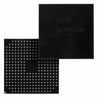
LPC3230FET296/01,5 NXP Semiconductors, LPC3230FET296/01,5 Datasheet - Page 9

LPC3230FET296/01,5
Manufacturer Part Number
LPC3230FET296/01,5
Description
IC ARM9 MCU 256K 296-TFBGA
Manufacturer
NXP Semiconductors
Series
LPC32x0r
Specifications of LPC3230FET296/01,5
Package / Case
296-TFBGA
Core Processor
ARM9
Core Size
16/32-Bit
Speed
266MHz
Connectivity
EBI/EMI, I²C, IrDA, Microwire, SPI, SSI, SSP, UART/USART, USB OTG
Peripherals
DMA, I²S, LCD, Motor Control PWM, PWM, WDT
Number Of I /o
51
Program Memory Type
ROMless
Ram Size
256K x 8
Voltage - Supply (vcc/vdd)
0.9 V ~ 3.6 V
Data Converters
A/D 3x10b
Oscillator Type
Internal
Operating Temperature
-40°C ~ 85°C
Processor Series
LPC32
Core
ARM926EJ-S
Data Bus Width
32 bit
Data Ram Size
256 KB
Interface Type
EMC
Maximum Clock Frequency
266 MHz
Number Of Timers
6
Operating Supply Voltage
1.31 V to 1.39 V
Maximum Operating Temperature
+ 85 C
Mounting Style
SMD/SMT
3rd Party Development Tools
MDK-ARM, RL-ARM, ULINK2
Minimum Operating Temperature
- 40 C
On-chip Adc
10 bit, 3 Channel
Lead Free Status / RoHS Status
Lead free / RoHS Compliant
Eeprom Size
-
Program Memory Size
-
Lead Free Status / Rohs Status
Lead free / RoHS Compliant
Other names
568-4964
935290764551
935290764551
Available stocks
Company
Part Number
Manufacturer
Quantity
Price
Company:
Part Number:
LPC3230FET296/01,5
Manufacturer:
NXP Semiconductors
Quantity:
10 000
NXP Semiconductors
ES_LPC3230
Errata sheet
2 inches of 50 Ω transmission line and 10 pF load capacitance. DDR memories specify
EMC_D[15:0] to EMC_DQS[1:0] set-up time minimum as 400 ps. This leaves 200 ps
set-up time margin due to customer specific load and PCB layout implementation. See the
LPC3220_30_40_50 data sheet for the complete range of DDR data output set-up time,
t
Work-around:
To get the most DDR set-up time margin, the following is recommended:
Example 128 MB system DDR SDRAM using a single EMC_DYCSx_N:
su(Q)
1. The DDR initialization software should set the SDRAMCLK_CTRL register (0x4000
2. Systems requiring 128 MB or less of DDR should be implemented using a single
3. Series termination resistors are not needed for the LPC3230 EMC outputs. If series
4. If the data bus EMC_D[15:0] is shared with additional devices (i.e., NOR flash,
5. The PCB trace length of EMC_DQS[1:0] should be at least 2 inches (but not more
4068) SDRAM_PIN_SPEED[3:1] bits = 0 (fast slew rate). This is for both 1.8 V mobile
and 2.5 V DDR memories.
EMC_DYCSx_N for DDR. The single chip select system may be constructed with a
single 16-bit wide DDR or two 8-bit wide DDR SDRAMs using up to the maximum
supported 512 Mbit DDR density. Using two 8-bit wide DDRs will have less capacitive
loading and facilitate simple point-to-point routing of EMC_D[15:0] and
EMC_DQS[1:0] signals over using two 16-bit DDRs and two EMC_DYCSx banks.
termination resistors are used they should be placed as close to the DDR
EMC_D[15:0] and EMC_DQS[1:0] pins as possible.
buffers, etc.) the board should be routed with a daisy chain topology, where the
LPC3230 is placed at one extreme of the data bus and the DDR(s) at the other
extreme. Other device(s) should be placed between the LPC3230 and DDR memory
(closer to the DDR).
than 4 inches) longer than EMC_DQ[15:0] and EMC_DQM[1:0]. On a typical FR4
PCB this adds at least 334 ps to set-up time margin for DDR writes. For reads from
DDR the increased trace length of EMC_DQS[1:0] will be automatically compensated
for by the software initialization function find_ddr_dqsin_delay() which sets the optimal
value DDR_DQSIN_DELAY(SDRAMCLK_CTRL[6:2]). The function
find_ddr_dqsin_delay() can be found in the "DDR SDRAM setup code for the
LPC32x0 series" on the NXP web site.
, and data output hold time t
All information provided in this document is subject to legal disclaimers.
Rev. 8 — 1 February 2011
h(Q)
times.
ES_LPC3230
Errata sheet LPC3230
© NXP B.V. 2011. All rights reserved.
9 of 17


