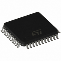
ST72F324LJ2T5 STMicroelectronics, ST72F324LJ2T5 Datasheet - Page 133

ST72F324LJ2T5
Manufacturer Part Number
ST72F324LJ2T5
Description
IC MCU 8BIT 8K FLASH 44-LQFP
Manufacturer
STMicroelectronics
Series
ST7r
Datasheet
1.ST72F324LJ2T5.pdf
(154 pages)
Specifications of ST72F324LJ2T5
Core Processor
ST7
Core Size
8-Bit
Speed
8MHz
Connectivity
SCI, SPI
Peripherals
POR, PWM, WDT
Number Of I /o
32
Program Memory Size
8KB (8K x 8)
Program Memory Type
FLASH
Ram Size
384 x 8
Voltage - Supply (vcc/vdd)
2.85 V ~ 3.6 V
Data Converters
A/D 12x10b
Oscillator Type
Internal
Operating Temperature
-10°C ~ 85°C
Package / Case
44-LQFP
Processor Series
ST72F3x
Core
ST7
Data Bus Width
8 bit
Data Ram Size
384 B
Interface Type
SCI, SPI
Maximum Clock Frequency
8 MHz
Number Of Programmable I/os
32
Number Of Timers
2
Maximum Operating Temperature
+ 85 C
Mounting Style
SMD/SMT
Development Tools By Supplier
ST7232X-EVAL, ST7MDT20-DVP3, ST7MDT20J-EMU3, STX-RLINK
Minimum Operating Temperature
- 10 C
On-chip Adc
10 bit, 12 Channel
For Use With
497-6421 - BOARD EVAL DGTL BATT CHGR DESIGN497-5046 - KIT TOOL FOR ST7/UPSD/STR7 MCU
Lead Free Status / RoHS Status
Lead free / RoHS Compliant
Eeprom Size
-
Lead Free Status / Rohs Status
Details
Other names
497-8242
ST72F324LJ2T5
ST72F324LJ2T5
Available stocks
Company
Part Number
Manufacturer
Quantity
Price
Company:
Part Number:
ST72F324LJ2T5
Manufacturer:
STMicroelectronics
Quantity:
10 000
Part Number:
ST72F324LJ2T5
Manufacturer:
ST
Quantity:
20 000
Company:
Part Number:
ST72F324LJ2T5TR
Manufacturer:
STMicroelectronics
Quantity:
10 000
ADC CHARACTERISTICS (Cont’d)
Figure 80. Typical A/D Converter Application
12.12.1 Analog Power Supply and Reference
Pins
Depending on the MCU pin count, the package
may feature separate V
power supply pins. These pins supply power to the
A/D converter cell and function as the high and low
reference voltages for the conversion. In some
packages, V
(refer to
alog supply and reference pads are internally
bonded to the V
Separation of the digital and analog power pins al-
low board designers to improve A/D performance.
Conversion accuracy can be impacted by voltage
drops and noise in the event of heavily loaded or
badly decoupled power supply lines (see
12.12.2 General PCB Design
12.12.2 General PCB Design Guidelines
To obtain best results, some general design and
layout rules should be followed when designing
the application PCB to shield the noise-sensitive,
analog physical interface from noise-generating
CMOS logic signals.
– Use separate digital and analog planes. The an-
alog ground plane should be connected to the
Section 2 on page
V
AIN
AREF
DD
and V
and V
R
AIN
SSA
SS
AREF
7). In this case the an-
pins.
pins are not available
C
Guidelines).
AIN
and V
AINx
SSA
Section
analog
V
DD
– Filter power to the analog power planes. It is rec-
– The analog and digital power supplies should be
– Properly place components and route the signal
V
0.6V
V
0.6V
digital ground plane via a single point on the
PCB.
ommended to connect capacitors, with good high
frequency characteristics, between the power
and ground lines, placing 0.1µF and optionally, if
needed 10pF capacitors as close as possible to
the ST7 power supply pins and a 1 to 10µF ca-
pacitor close to the power source (see
81).
connected in a star nework. Do not use a resis-
tor, as V
the A/D converter and any resistance would
cause a voltage drop and a loss of accuracy.
traces on the PCB to shield the analog inputs.
Analog signals paths should run over the analog
ground plane and be as short as possible. Isolate
analog signals from digital signals that may
switch while the analog inputs are being sampled
by the A/D converter. Do not toggle digital out-
puts on the same I/O port as the A/D input being
converted.
T
T
AREF
2kΩ(max)
I
±1µA
L
is used as a reference voltage by
10-Bit A/D
Conversion
ST72324Lxx
ST72XXX
Figure
C
12pF
133/154
ADC
1


