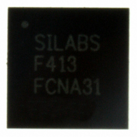
C8051F413-GM Silicon Laboratories Inc, C8051F413-GM Datasheet - Page 82

C8051F413-GM
Manufacturer Part Number
C8051F413-GM
Description
IC 8051 MCU 16K FLASH 28QFN
Manufacturer
Silicon Laboratories Inc
Series
C8051F41xr
Specifications of C8051F413-GM
Program Memory Type
FLASH
Program Memory Size
16KB (16K x 8)
Package / Case
28-QFN
Core Processor
8051
Core Size
8-Bit
Speed
50MHz
Connectivity
SMBus (2-Wire/I²C), SPI, UART/USART
Peripherals
Brown-out Detect/Reset, POR, PWM, Temp Sensor, WDT
Number Of I /o
20
Ram Size
2.25K x 8
Voltage - Supply (vcc/vdd)
2 V ~ 5.25 V
Data Converters
A/D 20x12b; D/A 2x12b
Oscillator Type
Internal
Operating Temperature
-40°C ~ 85°C
Processor Series
C8051F4x
Core
8051
Data Bus Width
8 bit
Data Ram Size
2.25 KB
Interface Type
I2C/SMBus/SPI/UART
Maximum Clock Frequency
50 MHz
Number Of Programmable I/os
20
Number Of Timers
4
Operating Supply Voltage
2 V to 5.25 V
Maximum Operating Temperature
+ 85 C
Mounting Style
SMD/SMT
3rd Party Development Tools
PK51, CA51, A51, ULINK2
Development Tools By Supplier
C8051F410DK
Minimum Operating Temperature
- 40 C
On-chip Dac
2-ch x 12-bit
Lead Free Status / RoHS Status
Lead free / RoHS Compliant
For Use With
770-1006 - ISP 4PORT FOR SILABS C8051F MCU336-1454 - ADAPTER PROGRAM TOOLSTICK F411336-1317 - KIT EVAL FOR C8051F411336-1314 - KIT DEV FOR C8051F41X
Eeprom Size
-
Lead Free Status / Rohs Status
Lead free / RoHS Compliant
Other names
336-1311
Available stocks
Company
Part Number
Manufacturer
Quantity
Price
Company:
Part Number:
C8051F413-GM
Manufacturer:
Silicon Labs
Quantity:
135
Part Number:
C8051F413-GM
Manufacturer:
SILICON LABS/èٹ¯ç§‘
Quantity:
20 000
Company:
Part Number:
C8051F413-GMR
Manufacturer:
M/A-COM
Quantity:
1 001
Part Number:
C8051F413-GMR
Manufacturer:
SILICON LABS/èٹ¯ç§‘
Quantity:
20 000
C8051F410/1/2/3
Table 8.1. Voltage Regulator Electrical Specifications
V
82
Input Voltage Range (V
Load Current
Load Regulation
Output Voltage (V
Bias Current
Dropout Indicator Detection
Threshold
Output Voltage Tempco
VREG Settling Time
*Note: Actual Output Voltage (V
DD
Bit 7:
Bit 6:
Bit 5:
Bit 4:
Bits 3–1: UNUSED. Read = 0b. Write = don’t care.
Bit 0:
REGDIS Reserved
= 2.1 or 2.5 V; –40 to +85 °C unless otherwise specified. Typical values are given at 25 ºC.
R/W
Bit7
Parameter
REGDIS: Voltage Regulator Disable Bit.
This bit disables/enables the Voltage Regulator.
0: Voltage Regulator Enabled.
1: Voltage Regulator Disabled.
RESERVED. Read = 0b. Must write 0b.
UNUSED. Read = 0b. Write = don’t care.
REG0MD: Voltage Regulator Mode Select Bit.
This bit selects the Voltage Regulator output voltage.
0: Voltage Regulator output is 2.1 V.
1: Voltage Regulator output is 2.5 V (default).
DROPOUT: Voltage Regulator Dropout Indicator Bit.
0: Voltage Regulator is not in dropout.
1: Voltage Regulator is in or near dropout.
R/W
Bit6
DD
)
SFR Definition 8.1. REG0CN: Regulator Control
REGIN
Bit5
—
)*
R
DD
) = Nominal Output Voltage (V
Output Current = 1 mA
REG0MD = ‘0’
REG0MD = ‘1’
REG0MD = ‘0’
REG0MD = ‘1’
50 mA load with V
and V
REG0MD
DD
R/W
Bit4
load capacitor of 4.8 µF
Conditions
Rev. 1.1
REGIN
Bit3
—
R
= 2.5 V
DD
) – (Load Regulation x Load Current).
Bit2
—
R
(See Note)
2.35
Min
2.0
—
—
—
—
—
—
—
Bit1
—
R
DROPOUT 00010000
Typ
600
250
SFR Address:
2.1
2.5
65
—
—
7
1
1
Bit0
R
Max
5.25
2.25
2.55
1.5
1.5
50
15
—
—
—
0xC9
Reset Value
mV/mA
µV/ºC
Units
mA
mV
µA
µs
V
V


