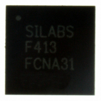
C8051F413-GM Silicon Laboratories Inc, C8051F413-GM Datasheet - Page 95

C8051F413-GM
Manufacturer Part Number
C8051F413-GM
Description
IC 8051 MCU 16K FLASH 28QFN
Manufacturer
Silicon Laboratories Inc
Series
C8051F41xr
Specifications of C8051F413-GM
Program Memory Type
FLASH
Program Memory Size
16KB (16K x 8)
Package / Case
28-QFN
Core Processor
8051
Core Size
8-Bit
Speed
50MHz
Connectivity
SMBus (2-Wire/I²C), SPI, UART/USART
Peripherals
Brown-out Detect/Reset, POR, PWM, Temp Sensor, WDT
Number Of I /o
20
Ram Size
2.25K x 8
Voltage - Supply (vcc/vdd)
2 V ~ 5.25 V
Data Converters
A/D 20x12b; D/A 2x12b
Oscillator Type
Internal
Operating Temperature
-40°C ~ 85°C
Processor Series
C8051F4x
Core
8051
Data Bus Width
8 bit
Data Ram Size
2.25 KB
Interface Type
I2C/SMBus/SPI/UART
Maximum Clock Frequency
50 MHz
Number Of Programmable I/os
20
Number Of Timers
4
Operating Supply Voltage
2 V to 5.25 V
Maximum Operating Temperature
+ 85 C
Mounting Style
SMD/SMT
3rd Party Development Tools
PK51, CA51, A51, ULINK2
Development Tools By Supplier
C8051F410DK
Minimum Operating Temperature
- 40 C
On-chip Dac
2-ch x 12-bit
Lead Free Status / RoHS Status
Lead free / RoHS Compliant
For Use With
770-1006 - ISP 4PORT FOR SILABS C8051F MCU336-1454 - ADAPTER PROGRAM TOOLSTICK F411336-1317 - KIT EVAL FOR C8051F411336-1314 - KIT DEV FOR C8051F41X
Eeprom Size
-
Lead Free Status / Rohs Status
Lead free / RoHS Compliant
Other names
336-1311
Available stocks
Company
Part Number
Manufacturer
Quantity
Price
Company:
Part Number:
C8051F413-GM
Manufacturer:
Silicon Labs
Quantity:
135
Part Number:
C8051F413-GM
Manufacturer:
SILICON LABS/èٹ¯ç§‘
Quantity:
20 000
Company:
Part Number:
C8051F413-GMR
Manufacturer:
M/A-COM
Quantity:
1 001
Part Number:
C8051F413-GMR
Manufacturer:
SILICON LABS/èٹ¯ç§‘
Quantity:
20 000
10.1.2. MOVX Instruction and Program Memory
The MOVX instruction is typically used to access data stored in XDATA memory space. In the CIP-51, the
MOVX instruction can also be used to write or erase on-chip program memory space implemented as re-
programmable Flash memory. The Flash access feature provides a mechanism for the CIP-51 to update
program code and use the program memory space for non-volatile data storage. Refer to
“16. Flash Memory” on page 135
ADD A, Rn
ADD A, direct
ADD A, @Ri
ADD A, #data
ADDC A, Rn
ADDC A, direct
ADDC A, @Ri
ADDC A, #data
SUBB A, Rn
SUBB A, direct
SUBB A, @Ri
SUBB A, #data
INC A
INC Rn
INC direct
INC @Ri
DEC A
DEC Rn
DEC direct
DEC @Ri
INC DPTR
MUL AB
DIV AB
DA A
ANL A, Rn
ANL A, direct
ANL A, @Ri
ANL A, #data
ANL direct, A
ANL direct, #data
ORL A, Rn
ORL A, direct
Notes:
1. Assumes PFEN = 1 for all instruction timing.
2. MOVC instructions take 4 to 7 clock cycles depending on instruction alignment and the FLRT setting (SFR
Definition 16.3. FLSCL: Flash Scale).
Mnemonic
Table 10.1. CIP-51 Instruction Set Summary
Add register to A
Add direct byte to A
Add indirect RAM to A
Add immediate to A
Add register to A with carry
Add direct byte to A with carry
Add indirect RAM to A with carry
Add immediate to A with carry
Subtract register from A with borrow
Subtract direct byte from A with borrow
Subtract indirect RAM from A with borrow
Subtract immediate from A with borrow
Increment A
Increment register
Increment direct byte
Increment indirect RAM
Decrement A
Decrement register
Decrement direct byte
Decrement indirect RAM
Increment Data Pointer
Multiply A and B
Divide A by B
Decimal adjust A
AND Register to A
AND direct byte to A
AND indirect RAM to A
AND immediate to A
AND A to direct byte
AND immediate to direct byte
OR Register to A
OR direct byte to A
for further details.
Arithmetic Operations
Logical Operations
Rev. 1.1
Description
C8051F410/1/2/3
1
Bytes
1
2
1
2
1
2
1
2
1
2
1
2
1
1
2
1
1
1
2
1
1
1
1
1
1
2
1
2
2
3
1
2
Cycles
Clock
Section
1
2
2
2
1
2
2
2
1
2
2
2
1
1
2
2
1
1
2
2
1
4
8
1
1
2
2
2
2
3
1
2
95


