MC56F8322MFAE Freescale Semiconductor, MC56F8322MFAE Datasheet - Page 16
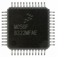
MC56F8322MFAE
Manufacturer Part Number
MC56F8322MFAE
Description
IC DSP 16BIT 60MHZ 48-LQFP
Manufacturer
Freescale Semiconductor
Series
56F8xxxr
Datasheet
1.MC56F8122VFAE.pdf
(136 pages)
Specifications of MC56F8322MFAE
Core Processor
56800
Core Size
16-Bit
Speed
60MHz
Connectivity
CAN, SCI, SPI
Peripherals
POR, PWM, Temp Sensor, WDT
Number Of I /o
21
Program Memory Size
40KB (20K x 16)
Program Memory Type
FLASH
Ram Size
6K x 16
Voltage - Supply (vcc/vdd)
2.25 V ~ 3.6 V
Data Converters
A/D 6x12b
Oscillator Type
Internal
Operating Temperature
-40°C ~ 125°C
Package / Case
48-LQFP
Cpu Family
56F8xxx
Device Core Size
16b
Frequency (max)
60MHz
Interface Type
CAN/SCI/SPI
Total Internal Ram Size
4KB
# I/os (max)
21
Number Of Timers - General Purpose
2
Operating Supply Voltage (typ)
2.5/3.3V
Operating Supply Voltage (max)
2.75/3.6V
Operating Supply Voltage (min)
2.25/3V
On-chip Adc
2(3-chx12-bit)
Instruction Set Architecture
CISC
Operating Temp Range
-40C to 125C
Operating Temperature Classification
Automotive
Mounting
Surface Mount
Pin Count
48
Package Type
LQFP
Data Bus Width
16 bit
Processor Series
MC56F83xx
Core
56800E
Numeric And Arithmetic Format
Fixed-Point
Device Million Instructions Per Second
40 MIPs
Maximum Clock Frequency
60 MHz
Number Of Programmable I/os
21
Data Ram Size
4 KB
Operating Supply Voltage
- 0.3 V to + 4 V
Maximum Operating Temperature
+ 125 C
Mounting Style
SMD/SMT
Data Rom Size
8 KB
Minimum Operating Temperature
- 40 C
For Use With
MC56F8323EVME - BOARD EVALUATION MC56F8323
Lead Free Status / RoHS Status
Lead free / RoHS Compliant
Eeprom Size
-
Lead Free Status / Rohs Status
Compliant
Available stocks
Company
Part Number
Manufacturer
Quantity
Price
Company:

Part Number:
MC56F8322MFAE
Manufacturer:
VISHAY
Quantity:
12 500
Company:
Part Number:
MC56F8322MFAE
Manufacturer:
Freescale Semiconductor
Quantity:
10 000
Part Number:
MC56F8322MFAE
Manufacturer:
FREESCALE
Quantity:
20 000


Part 2 Signal/Connection Descriptions
2.1 Introduction
The input and output signals of the 56F8322 and 56F8122 devices are organized into functional groups,
as detailed in
describes the signal or signals present on a pin.
Note: See
16
1. The V
2. Pins in this section can function as SPI #1 and GPIO.
3. Pins in this section can function as SCI #1 and GPIO.
4. Alternately, can function as Quad Timer A pins or GPIO.
5. Pins can function as SCI #0 and GPIO.
6. Tied internally to ANA7
Power (V
Ground (V
Supply Capacitors & V
PLL and Clock
Interrupt and Program Control
Pulse Width Modulator (PWM) Ports
Serial Peripheral Interface (SPI) Port 0
Quadrature Decoder Port 0
CAN Ports
Analog to Digital Converter (ADC) Ports
Timer Module Port C
Timer Module Port A
JTAG/Enhanced On-Chip Emulation (EOnCE)
Temperature Sense
Dedicated GPIO
Table 1-1
PP
Table 2-1
DD
input shares the IRQA input
SS
for 56F8122 functional differences.
or V
or V
DDA
SSA
Functional Group
6
)
5
)
and as illustrated in
PP
Table 2-1 Functional Group Pin Allocations
1
4
2
56F8322 Techncial Data, Rev. 16
3
Figure 2-1
and
Figure
56F8322
—
—
Number of Pins in Package
5
5
2
2
2
7
4
4
2
9
2
4
0
2-2. In
Table
2-2, each table row
Freescale Semiconductor
56F8122
—
—
—
—
5
5
2
2
2
8
9
2
4
4
5
Preliminary
Related parts for MC56F8322MFAE
Image
Part Number
Description
Manufacturer
Datasheet
Request
R

Part Number:
Description:
Manufacturer:
Freescale Semiconductor, Inc
Datasheet:
Part Number:
Description:
Manufacturer:
Freescale Semiconductor, Inc
Datasheet:
Part Number:
Description:
Manufacturer:
Freescale Semiconductor, Inc
Datasheet:
Part Number:
Description:
Manufacturer:
Freescale Semiconductor, Inc
Datasheet:
Part Number:
Description:
Manufacturer:
Freescale Semiconductor, Inc
Datasheet:
Part Number:
Description:
Manufacturer:
Freescale Semiconductor, Inc
Datasheet:
Part Number:
Description:
Manufacturer:
Freescale Semiconductor, Inc
Datasheet:
Part Number:
Description:
Manufacturer:
Freescale Semiconductor, Inc
Datasheet:
Part Number:
Description:
Manufacturer:
Freescale Semiconductor, Inc
Datasheet:
Part Number:
Description:
Manufacturer:
Freescale Semiconductor, Inc
Datasheet:
Part Number:
Description:
Manufacturer:
Freescale Semiconductor, Inc
Datasheet:
Part Number:
Description:
Manufacturer:
Freescale Semiconductor, Inc
Datasheet:
Part Number:
Description:
Manufacturer:
Freescale Semiconductor, Inc
Datasheet:
Part Number:
Description:
Manufacturer:
Freescale Semiconductor, Inc
Datasheet:
Part Number:
Description:
Manufacturer:
Freescale Semiconductor, Inc
Datasheet: