DF2338VFC25V Renesas Electronics America, DF2338VFC25V Datasheet - Page 176
DF2338VFC25V
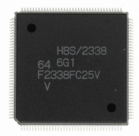
Manufacturer Part Number
DF2338VFC25V
Description
IC H8S/2300 MCU FLASH 144QFP
Manufacturer
Renesas Electronics America
Series
H8® H8S/2300r
Datasheets
1.HEWH8E10A.pdf
(19 pages)
2.D12312SVTE25V.pdf
(341 pages)
3.DF2338VFC25V.pdf
(1246 pages)
Specifications of DF2338VFC25V
Core Processor
H8S/2000
Core Size
16-Bit
Speed
25MHz
Connectivity
SCI, SmartCard
Peripherals
DMA, POR, PWM, WDT
Number Of I /o
106
Program Memory Size
256KB (256K x 8)
Program Memory Type
FLASH
Ram Size
8K x 8
Voltage - Supply (vcc/vdd)
2.7 V ~ 3.6 V
Data Converters
A/D 12x10b; D/A 4x8b
Oscillator Type
Internal
Operating Temperature
-20°C ~ 75°C
Package / Case
144-QFP
For Use With
EDK2329 - DEV EVALUATION KIT H8S/2329
Lead Free Status / RoHS Status
Lead free / RoHS Compliant
Eeprom Size
-
Available stocks
Company
Part Number
Manufacturer
Quantity
Price
Company:

Part Number:
DF2338VFC25V
Manufacturer:
Renesas Electronics America
Quantity:
10 000


6.2.6
MCR is an 8-bit readable/writable register that selects the DRAM strobe control method, number
of precharge cycles, access mode, address multiplexing shift size, and the number of wait states
inserted during refreshing, when areas 2 to 5 are designated as DRAM interface areas.
MCR is initialized to H'00 by a reset, and in hardware standby mode. It is not initialized in
software standby mode.
Bit 7—TP Cycle Control (TPC): Selects whether a 1-state or 2-state precharge cycle (T
used when areas 2 to 5 designated as DRAM space are accessed.
Bit 7
TPC
0
1
Bit 6—Burst Access Enable (BE): Selects enabling or disabling of burst access to areas 2 to 5
designated as DRAM space. DRAM space burst access is performed in fast page mode.
Bit 6
BE
0
1
Bit 5—RAS Down Mode (RCDM): When areas 2 to 5 are designated as DRAM space and
access to DRAM is interrupted, RCDM selects whether the RAS signal is held low while waiting
for the next DRAM access (RAS down mode), or is driven high again (RAS up mode).
Bit 5
RCDM
0
1
Rev.4.00 Sep. 07, 2007 Page 144 of 1210
REJ09B0245-0400
Bit
Initial value :
R/W
Memory Control Register (MCR)
:
:
Description
1-state precharge cycle is inserted
2-state precharge cycle is inserted
Description
Burst disabled (always full access)
DRAM space access performed in fast page mode
Description
RAS up mode selected for DRAM interface
RAS down mode selected for DRAM interface
TPC
R/W
7
0
R/W
BE
6
0
RCDM
R/W
5
0
R/W
—
4
0
MXC1
R/W
0
3
MXC0
R/W
2
0
RLW1
R/W
1
0
(Initial value)
(Initial value)
(Initial value)
P
) is to be
RLW0
R/W
0
0
Related parts for DF2338VFC25V
Image
Part Number
Description
Manufacturer
Datasheet
Request
R

Part Number:
Description:
KIT STARTER FOR M16C/29
Manufacturer:
Renesas Electronics America
Datasheet:

Part Number:
Description:
KIT STARTER FOR R8C/2D
Manufacturer:
Renesas Electronics America
Datasheet:

Part Number:
Description:
R0K33062P STARTER KIT
Manufacturer:
Renesas Electronics America
Datasheet:

Part Number:
Description:
KIT STARTER FOR R8C/23 E8A
Manufacturer:
Renesas Electronics America
Datasheet:

Part Number:
Description:
KIT STARTER FOR R8C/25
Manufacturer:
Renesas Electronics America
Datasheet:

Part Number:
Description:
KIT STARTER H8S2456 SHARPE DSPLY
Manufacturer:
Renesas Electronics America
Datasheet:

Part Number:
Description:
KIT STARTER FOR R8C38C
Manufacturer:
Renesas Electronics America
Datasheet:

Part Number:
Description:
KIT STARTER FOR R8C35C
Manufacturer:
Renesas Electronics America
Datasheet:

Part Number:
Description:
KIT STARTER FOR R8CL3AC+LCD APPS
Manufacturer:
Renesas Electronics America
Datasheet:
Part Number:
Description:
KIT STARTER FOR RX610
Manufacturer:
Renesas Electronics America
Datasheet:

Part Number:
Description:
KIT STARTER FOR R32C/118
Manufacturer:
Renesas Electronics America
Datasheet:

Part Number:
Description:
KIT DEV RSK-R8C/26-29
Manufacturer:
Renesas Electronics America
Datasheet:

Part Number:
Description:
KIT STARTER FOR SH7124
Manufacturer:
Renesas Electronics America
Datasheet:

Part Number:
Description:
KIT STARTER FOR H8SX/1622
Manufacturer:
Renesas Electronics America
Datasheet:

Part Number:
Description:
KIT DEV FOR SH7203
Manufacturer:
Renesas Electronics America
Datasheet: