DF2338VFC25V Renesas Electronics America, DF2338VFC25V Datasheet - Page 692
DF2338VFC25V
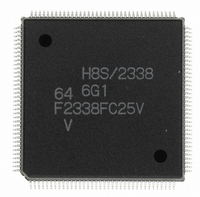
Manufacturer Part Number
DF2338VFC25V
Description
IC H8S/2300 MCU FLASH 144QFP
Manufacturer
Renesas Electronics America
Series
H8® H8S/2300r
Datasheets
1.HEWH8E10A.pdf
(19 pages)
2.D12312SVTE25V.pdf
(341 pages)
3.DF2338VFC25V.pdf
(1246 pages)
Specifications of DF2338VFC25V
Core Processor
H8S/2000
Core Size
16-Bit
Speed
25MHz
Connectivity
SCI, SmartCard
Peripherals
DMA, POR, PWM, WDT
Number Of I /o
106
Program Memory Size
256KB (256K x 8)
Program Memory Type
FLASH
Ram Size
8K x 8
Voltage - Supply (vcc/vdd)
2.7 V ~ 3.6 V
Data Converters
A/D 12x10b; D/A 4x8b
Oscillator Type
Internal
Operating Temperature
-20°C ~ 75°C
Package / Case
144-QFP
For Use With
EDK2329 - DEV EVALUATION KIT H8S/2329
Lead Free Status / RoHS Status
Lead free / RoHS Compliant
Eeprom Size
-
Available stocks
Company
Part Number
Manufacturer
Quantity
Price
Company:

Part Number:
DF2338VFC25V
Manufacturer:
Renesas Electronics America
Quantity:
10 000


Operation in Case of Mode Transition
• Transmission
• Reception
Rev.4.00 Sep. 07, 2007 Page 660 of 1210
REJ09B0245-0400
Operation should be stopped (by clearing TE, TIE, and TEIE to 0) before making a module
stop mode or software standby mode transition. TSR, TDR, and SSR are reset. The output pin
states in module stop mode or software standby mode depend on the port settings, and
becomes high-level output after the relevant mode is cleared. If a transition is made during
transmission, the data being transmitted will be undefined. When transmitting without
changing the transmit mode after the relevant mode is cleared, transmission can be started by
setting TE to 1 again, and performing the following sequence: SSR read → TDR write →
TDRE clearance. To transmit with a different transmit mode after clearing the relevant mode,
the procedure must be started again from initialization. Figure 14.23 shows a sample flowchart
for mode transition during transmission. Port pin states are shown in figures 14.24 and 14.25.
Operation should also be stopped (by clearing TE, TIE, and TEIE to 0) before making a
transition from transmission by DTC transfer to module stop mode or software standby mode
transition. To perform transmission with the DTC after the relevant mode is cleared, setting TE
and TIE to 1 will set the TXI flag and start DTC transmission.
Receive operation should be stopped (by clearing RE to 0) before making a module stop mode
or software standby mode transition. RSR, RDR, and SSR are reset. If a transition is made
without stopping operation, the data being received will be invalid.
To continue receiving without changing the reception mode after the relevant mode is cleared,
set RE to 1 before starting reception. To receive with a different receive mode, the procedure
must be started again from initialization.
Figure 14.26 shows a sample flowchart for mode transition during reception.
Related parts for DF2338VFC25V
Image
Part Number
Description
Manufacturer
Datasheet
Request
R

Part Number:
Description:
KIT STARTER FOR M16C/29
Manufacturer:
Renesas Electronics America
Datasheet:

Part Number:
Description:
KIT STARTER FOR R8C/2D
Manufacturer:
Renesas Electronics America
Datasheet:

Part Number:
Description:
R0K33062P STARTER KIT
Manufacturer:
Renesas Electronics America
Datasheet:

Part Number:
Description:
KIT STARTER FOR R8C/23 E8A
Manufacturer:
Renesas Electronics America
Datasheet:

Part Number:
Description:
KIT STARTER FOR R8C/25
Manufacturer:
Renesas Electronics America
Datasheet:

Part Number:
Description:
KIT STARTER H8S2456 SHARPE DSPLY
Manufacturer:
Renesas Electronics America
Datasheet:

Part Number:
Description:
KIT STARTER FOR R8C38C
Manufacturer:
Renesas Electronics America
Datasheet:

Part Number:
Description:
KIT STARTER FOR R8C35C
Manufacturer:
Renesas Electronics America
Datasheet:

Part Number:
Description:
KIT STARTER FOR R8CL3AC+LCD APPS
Manufacturer:
Renesas Electronics America
Datasheet:
Part Number:
Description:
KIT STARTER FOR RX610
Manufacturer:
Renesas Electronics America
Datasheet:

Part Number:
Description:
KIT STARTER FOR R32C/118
Manufacturer:
Renesas Electronics America
Datasheet:

Part Number:
Description:
KIT DEV RSK-R8C/26-29
Manufacturer:
Renesas Electronics America
Datasheet:

Part Number:
Description:
KIT STARTER FOR SH7124
Manufacturer:
Renesas Electronics America
Datasheet:

Part Number:
Description:
KIT STARTER FOR H8SX/1622
Manufacturer:
Renesas Electronics America
Datasheet:

Part Number:
Description:
KIT DEV FOR SH7203
Manufacturer:
Renesas Electronics America
Datasheet: