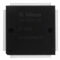
SAK-C167CS-LM CA+ Infineon Technologies, SAK-C167CS-LM CA+ Datasheet - Page 64

SAK-C167CS-LM CA+
Manufacturer Part Number
SAK-C167CS-LM CA+
Description
IC MCU 16BIT 25MHZ MQFP-144
Manufacturer
Infineon Technologies
Series
C16xxr
Datasheet
1.SAK-C167CS-LM_CA.pdf
(81 pages)
Specifications of SAK-C167CS-LM CA+
Core Processor
C166
Core Size
16-Bit
Speed
25MHz
Connectivity
CAN, EBI/EMI, SPI, SSC, UART/USART
Peripherals
POR, PWM, WDT
Number Of I /o
111
Program Memory Type
ROMless
Ram Size
11K x 8
Voltage - Supply (vcc/vdd)
4.5 V ~ 5.5 V
Data Converters
A/D 24x10b
Oscillator Type
External
Operating Temperature
-40°C ~ 125°C
Package / Case
144- BSQFP
Packages
PG-MQFP-144
Max Clock Frequency
25.0 MHz
Sram (incl. Cache)
11.0 KByte
Can Nodes
2
A / D Input Lines (incl. Fadc)
24
Program Memory
0.0 KByte
Lead Free Status / RoHS Status
Lead free / RoHS Compliant
Eeprom Size
-
Program Memory Size
-
Other names
K167CSLMCAZNP
K167CSLMCAZXP
K167CSLMCAZXT
SAK-C167CS-LM CA+
SAK-C167CS-LMCAIN
SAKC167CSLMCAT
SP000103492
K167CSLMCAZXP
K167CSLMCAZXT
SAK-C167CS-LM CA+
SAK-C167CS-LMCAIN
SAKC167CSLMCAT
SP000103492
A/D Converter Characteristics
(Operating Conditions apply)
Table 13
Parameter
Analog reference supply
Analog reference ground
Analog input voltage range
Basic clock frequency
Conversion time
Calibration time after reset
Total unadjusted error
Internal resistance of
reference voltage source
Internal resistance of
analog source
ADC input capacitance
1)
2)
3)
4)
Data Sheet
TUE is tested at
within the defined voltage range.
If the analog reference supply voltage exceeds the power supply voltage by up to 0.2 V
(i.e.
The specified TUE is guaranteed only if the absolute sum of input overload currents on Port 5 pins and P1H
pins (see
During the reset calibration sequence the maximum TUE may be ±4 LSB (±12 LSB for channels 16 … 23).
V
these cases will be X000
The limit values for
This parameter includes the sample time
result register with the conversion result.
Values for the basic clock
This parameter depends on the ADC control logic. It is not a real maximum value, but rather a fixum.
AIN
V
may exceed
AREF
I
OV
=
V
specification) does not exceed 10 mA.
DD
A/D Converter Characteristics
V
= +0.2 V) the maximum TUE is increased to ±3/11 LSB. This range is not 100% tested.
AREF
V
f
AGND
BC
must not be exceeded when selecting the CPU frequency and the ADCTC setting.
= 5.0 V,
H
or
t
or X3FF
BC
V
depend on programming and can be taken from
AREF
V
Symbol
V
V
V
f
t
t
TUE
R
R
C
AGND
BC
C
CAL
H
AREF
AGND
AIN
AREF
ASRC
AIN
up to the absolute maximum ratings. However, the conversion result in
, respectively.
= 0 V,
t
S
SR
SR
SR
CC
CC
CC
SR
SR
CC
, the time for determining the digital result and the time to load the
1)
V
DD
min.
4.0
V
V
0.5
–
–
–
–
–
–
–
60
= 4.9 V. It is guaranteed by design for all other voltages
SS
AGND
Limit Values
- 0.1
max.
V
V
V
6.25
40
+ 2
3328
± 2
± 10
t
- 0.25
t
- 0.25
33
BC
S
DD
SS
AREF
/450
t
t
/60
BC
CPU
+ 0.2
+ 0.1
t
BC
+
t
S
Table
Unit Test
V
V
V
MHz
–
–
LSB Channels
LSB Channels
k Ω
k Ω
pF
14.
Condition
1)
–
2)
3)
4)
t
5)
0 … 15
16 … 23
t
t
7)
CPU
BC
S
C167CS-4R
V2.2, 2001-08
C167CS-L
in [ns]
in [ns]
= 1/
7)8)
f
CPU
6)7)


