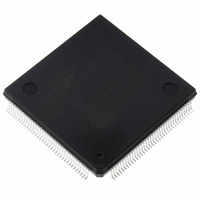
ST10F272Z2Q3 STMicroelectronics, ST10F272Z2Q3 Datasheet - Page 12

ST10F272Z2Q3
Manufacturer Part Number
ST10F272Z2Q3
Description
MCU 16BIT 256KB FLASH 144-PQFP
Manufacturer
STMicroelectronics
Series
ST10r
Datasheet
1.ST10F272Z2Q3.pdf
(189 pages)
Specifications of ST10F272Z2Q3
Core Processor
ST10
Core Size
16-Bit
Speed
64MHz
Connectivity
ASC, CAN, EBI/EMI, I²C, SSC, UART/USART
Peripherals
POR, PWM, WDT
Number Of I /o
111
Program Memory Size
256KB (256K x 8)
Program Memory Type
FLASH
Ram Size
20K x 8
Voltage - Supply (vcc/vdd)
4.5 V ~ 5.5 V
Data Converters
A/D 24x10b
Oscillator Type
Internal
Operating Temperature
-40°C ~ 125°C
Package / Case
144-QFP
Lead Free Status / RoHS Status
Lead free / RoHS Compliant
Eeprom Size
-
Other names
497-5579
Available stocks
Company
Part Number
Manufacturer
Quantity
Price
Company:
Part Number:
ST10F272Z2Q3
Manufacturer:
E-CMOS
Quantity:
10 000
Company:
Part Number:
ST10F272Z2Q3
Manufacturer:
STMicroelectronics
Quantity:
10 000
- Current page: 12 of 189
- Download datasheet (4Mb)
Description
12/189
CLKOUT function can output either the CPU clock (like in ST10F269) or a software
programmable prescaled value of the CPU clock.
On-chip RAM memory has been increased (Flash size remained the same).
PLL multiplication factors have been adapted to new frequency range.
A/D Converter is not fully compatible versus ST10F269 (timing and programming model).
Formula for the convertion time is still valid, while the sampling phase programming model is
different.
Besides, additional 8 channels are available on P1L pins as alternate function: the accuracy
reachable with these extra channels is reduced with respect to the standard Port5 channels.
External Memory bus is affected by limitations on maximum speed and maximum
capacitance load: ST10F272Z2 is not able to address an external memory at 64 MHz with 0
wait states.
XPERCON register bit mapping modified according to new peripherals implementation (not
fully compatible with ST10F269).
Bondout chip for emulation (ST10R201) cannot achieve more than 50 MHz at room
temperature (so no real-time emulation possible at maximum speed).
Input section characteristics are different. The threshold programmability is extended to all
port pins (additional XPICON register); it is possible to select standard TTL (with up to
400mV of hysteresis) and standard CMOS (with up to 750 mV of hysteresis).
Output transition is not programmable.
CAN module is enhanced: ST10F272Z2 implements two C-CAN modules, so the
programming model is slightly different. Besides, the possibility to map in parallel the two
CAN modules is added (on P4.5/P4.6).
On-chip main oscillator input frequency range has been reshaped, reducing it from
1-25 MHz down to 4-8 MHz. This is a low power oscillator amplifier, that allows a power
consumption reduction when Real-Time Clock is running in Power Down mode, using as
reference the on-chip main oscillator clock. When this on-chip amplifier is used as reference
for Real-Time Clock module, the Power-down consumption is dominated by the
consumption of the oscillator amplifier itself.
A second on-chip oscillator amplifier circuit (32 kHz) is implemented for low power modes: it
can be used to provide the reference to the Real-Time Clock counter (either in Power Down
or Stand-by mode). Pin XTAL3 and XTAL4 replace a couple of VDD/VSS pins of ST10F269.
Possibility to re-program internal XBUS chip select window characteristics (XRAM2 window)
is added.
ST10F272Z2
Related parts for ST10F272Z2Q3
Image
Part Number
Description
Manufacturer
Datasheet
Request
R

Part Number:
Description:
STMicroelectronics [RIPPLE-CARRY BINARY COUNTER/DIVIDERS]
Manufacturer:
STMicroelectronics
Datasheet:

Part Number:
Description:
STMicroelectronics [LIQUID-CRYSTAL DISPLAY DRIVERS]
Manufacturer:
STMicroelectronics
Datasheet:

Part Number:
Description:
BOARD EVAL FOR MEMS SENSORS
Manufacturer:
STMicroelectronics
Datasheet:

Part Number:
Description:
NPN TRANSISTOR POWER MODULE
Manufacturer:
STMicroelectronics
Datasheet:

Part Number:
Description:
TURBOSWITCH ULTRA-FAST HIGH VOLTAGE DIODE
Manufacturer:
STMicroelectronics
Datasheet:

Part Number:
Description:
Manufacturer:
STMicroelectronics
Datasheet:

Part Number:
Description:
DIODE / SCR MODULE
Manufacturer:
STMicroelectronics
Datasheet:

Part Number:
Description:
DIODE / SCR MODULE
Manufacturer:
STMicroelectronics
Datasheet:

Part Number:
Description:
Search -----> STE16N100
Manufacturer:
STMicroelectronics
Datasheet:

Part Number:
Description:
Search ---> STE53NA50
Manufacturer:
STMicroelectronics
Datasheet:

Part Number:
Description:
NPN Transistor Power Module
Manufacturer:
STMicroelectronics
Datasheet:


