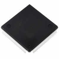
ST10F272Z2Q3 STMicroelectronics, ST10F272Z2Q3 Datasheet - Page 23

ST10F272Z2Q3
Manufacturer Part Number
ST10F272Z2Q3
Description
MCU 16BIT 256KB FLASH 144-PQFP
Manufacturer
STMicroelectronics
Series
ST10r
Datasheet
1.ST10F272Z2Q3.pdf
(189 pages)
Specifications of ST10F272Z2Q3
Core Processor
ST10
Core Size
16-Bit
Speed
64MHz
Connectivity
ASC, CAN, EBI/EMI, I²C, SSC, UART/USART
Peripherals
POR, PWM, WDT
Number Of I /o
111
Program Memory Size
256KB (256K x 8)
Program Memory Type
FLASH
Ram Size
20K x 8
Voltage - Supply (vcc/vdd)
4.5 V ~ 5.5 V
Data Converters
A/D 24x10b
Oscillator Type
Internal
Operating Temperature
-40°C ~ 125°C
Package / Case
144-QFP
Lead Free Status / RoHS Status
Lead free / RoHS Compliant
Eeprom Size
-
Other names
497-5579
Available stocks
Company
Part Number
Manufacturer
Quantity
Price
Company:
Part Number:
ST10F272Z2Q3
Manufacturer:
E-CMOS
Quantity:
10 000
Company:
Part Number:
ST10F272Z2Q3
Manufacturer:
STMicroelectronics
Quantity:
10 000
ST10F272Z2
Memory organization
After reset the XRAM2 is mapped from address 09’0000h.
XRAM2 represents also the Stand-by RAM, which can be maintained biased through EA /
VSTBY pin when main supply VDD is turned off.
As the XRAM appears like external memory, it cannot be used as system stack or as
register banks. The XRAM is not provided for single bit storage and therefore is not bit
addressable.
ST10F272 XRAM: 16K+2K Bytes of XRAM
The XRAM1 (2K Bytes) address range is 00’E000h - 00’E7FFh if enabled.
The XRAM2 (16K Bytes) address range is after reset 09’0000h - 09’3FFFh and is mirrored
every 16KByte boundary.
SFR/ESFR: 1024 Bytes (2 x 512 Bytes) of address space is reserved for the special
function register areas. SFRs are Wordwide registers which are used to control and to
monitor the function of the different on-chip units.
CAN1: Address range 00’EF00h - 00’EFFFh is reserved for the CAN1 Module access. The
CAN1 is enabled by setting XPEN bit 2 of the SYSCON register and by setting CAN1EN bit
0 of the XPERCON register. Accesses to the CAN Module use demultiplexed addresses
and a 16-bit data bus (only word accesses are possible). Two wait states give an access
time of 62.5ns at 64 MHz CPU clock. No tri-state wait states are used.
CAN2: Address range 00’EE00h - 00’EEFFh is reserved for the CAN2 Module access. The
CAN2 is enabled by setting XPEN bit 2 of the SYSCON register and by setting CAN2EN bit
1 of the new XPERCON register. Accesses to the CAN Module use demultiplexed
addresses and a 16-bit data bus (only word accesses are possible). Two wait states give an
access time of 62.5ns at 64 MHz CPU clock. No tri-state wait states are used.
If one or the two CAN modules are used, Port 4 cannot be programmed to output all 8
segment address lines. Thus, only 4 segment address lines can be used, reducing the
external memory space to 5 Mbytes (1 Mbyte per CS line).
RTC: Address range 00’ED00h - 00’EDFFh is reserved for the RTC Module access. The
RTC is enabled by setting XPEN bit 2 of the SYSCON register and bit 4 of the XPERCON
register. Accesses to the RTC Module use demultiplexed addresses and a 16-bit data bus
(only word accesses are possible). Two waitstates give an access time of 62.5ns at 64MHz
CPU clock. No tristate waitstate is used.
PWM1: Address range 00’EC00h - 00’ECFFh is reserved for the PWM1 Module access.
The PWM1 is enabled by setting XPEN bit 2 of the SYSCON register and bit 6 of the
XPERCON register. Accesses to the PWM1 Module use demultiplexed addresses and a 16-
bit data bus (only word accesses are possible). Two waitstates give an access time of
62.5 ns at 64 MHz CPU clock. No tristate waitstate is used. Only word access is allowed.
ASC1: Address range 00’E900h - 00’E9FFh is reserved for the ASC1 Module access. The
ASC1 is enabled by setting XPEN bit 2 of the SYSCON register and bit 7 of the XPERCON
register. Accesses to the ASC1 Module use demultiplexed addresses and a 16-bit data bus
(only word accesses are possible). Two waitstates give an access time of 62.5 ns at 64MHz
CPU clock. No tristate waitstate is used.
SSC1: Address range 00’E800h - 00’E8FFh is reserved for the SSC1 Module access. The
SSC1 is enabled by setting XPEN bit 2 of the SYSCON register and bit 8 of the XPERCON
register. Accesses to the SSC1 Module use demultiplexed addresses and a 16-bit data bus
23/189


