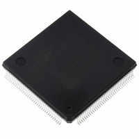
ST10F272Z2Q3 STMicroelectronics, ST10F272Z2Q3 Datasheet - Page 152

ST10F272Z2Q3
Manufacturer Part Number
ST10F272Z2Q3
Description
MCU 16BIT 256KB FLASH 144-PQFP
Manufacturer
STMicroelectronics
Series
ST10r
Datasheet
1.ST10F272Z2Q3.pdf
(189 pages)
Specifications of ST10F272Z2Q3
Core Processor
ST10
Core Size
16-Bit
Speed
64MHz
Connectivity
ASC, CAN, EBI/EMI, I²C, SSC, UART/USART
Peripherals
POR, PWM, WDT
Number Of I /o
111
Program Memory Size
256KB (256K x 8)
Program Memory Type
FLASH
Ram Size
20K x 8
Voltage - Supply (vcc/vdd)
4.5 V ~ 5.5 V
Data Converters
A/D 24x10b
Oscillator Type
Internal
Operating Temperature
-40°C ~ 125°C
Package / Case
144-QFP
Lead Free Status / RoHS Status
Lead free / RoHS Compliant
Eeprom Size
-
Other names
497-5579
Available stocks
Company
Part Number
Manufacturer
Quantity
Price
Company:
Part Number:
ST10F272Z2Q3
Manufacturer:
E-CMOS
Quantity:
10 000
Company:
Part Number:
ST10F272Z2Q3
Manufacturer:
STMicroelectronics
Quantity:
10 000
Electrical characteristics
152/189
●
The two transients above are not influenced by the voltage source that, due to the presence
of the R
C
respect to the sampling time (T
Figure
Calling f
the anti-aliasing filter, f
least 2f
the conversion period (T
T
selected (fastest conversion rate at a specific channel): in conclusion it is evident that the
time constant of the filter R
charge level on C
the sampling switch is closed.
S
S
, which is just a portion of it, even when fixed channel continuous conversion mode is
with respect to the ideal source V
This relation can again be simplified considering only C
condition. In reality, the transient is faster, but the A/D Converter circuitry has been
designed to be robust also in the very worst case: the sampling time T
longer than the internal time constant:
The charge of C
voltage V
A second charge transfer involves also C
capacitance) through the resistance R
and C
time constant is:
In this case, the time constant depends on the external circuit: in particular imposing
that the transient is completed well before the end of sampling time T
R
Of course, R
combination with R
definitively bigger than C
charge transfer transient) will be much higher than V
respected (charge balance assuming now C
L
45).
0
F
sizing is obtained:
0
; it means that the constant time of the filter is greater than or at least equal to twice
C
the bandwidth of the source signal (and as a consequence the cut-off frequency of
F
S
filter, is not able to provide the extra charge to compensate the voltage drop on
were in parallel to C
A1
on the capacitance according to the following equation:
V A2 C S C P1 C P2 C F
S
L
shall be sized also according to the current limitation constraints, in
cannot be modified by the analog signal source during the time in which
P1
⋅
(
F
), according to Nyquist theorem the conversion rate f
and C
S
C
V A1
). Again the conversion period T
+
10 τ 2
(source impedance) and R
F
τ 1
C
⋅
⋅
P1
F
<
P2
(
C S
S
is definitively much higher than the sampling time T
(
+
, C
=
). The filter is typically designed to act as anti-aliasing (see
R SW
P1
is redistributed also on C
τ 2 R L
10 R
+
P2
<
(since the time constant in reality would be faster), the
C P1
A
⋅ L
and C
+
+
; the time constant R
R AD
⋅
+
⋅
(
C S
(
C P2
)
L
C S
S
=
: again considering the worst case in which C
)
, then the final voltage V
V A C F
⋅
+
F
C S
+
)
C P1
(that is typically bigger than the on-chip
⋅
C P1
=
S
< <
V A
already charged at V
+
+
F
+
V A1
C P2
⋅
(filter resistance). Being C
C P2
T
(
C P1
S
A1
⋅
C
(
S
)
C P1 C P2
F
)
. The following equation must be
, determining a new value of the
is longer than the sampling time
C
≤
S
+
F
as an additional worst
C P2
T S
+
of the filter is very high with
)
A2
+
C S
(at the end of the
A1
S
)
):
S
, a constraints on
is always much
C
must be at
ST10F272Z2
F
S
, so the
P2


