C8051F901-GU Silicon Laboratories Inc, C8051F901-GU Datasheet - Page 11
C8051F901-GU
Manufacturer Part Number
C8051F901-GU
Description
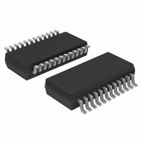
IC MCU 8BIT 8KB FLASH 24QSOP
Manufacturer
Silicon Laboratories Inc
Series
C8051F9xxr
Specifications of C8051F901-GU
Program Memory Type
FLASH
Program Memory Size
8KB (8K x 8)
Package / Case
24-QSOP
Core Processor
8051
Core Size
8-Bit
Speed
25MHz
Connectivity
SMBus (2-Wire/I²C), SPI, UART/USART
Peripherals
Brown-out Detect/Reset, POR, PWM, Temp Sensor, WDT
Number Of I /o
16
Ram Size
768 x 8
Voltage - Supply (vcc/vdd)
0.9 V ~ 3.6 V
Data Converters
A/D 15x10b
Oscillator Type
Internal
Operating Temperature
-40°C ~ 85°C
Processor Series
C8051F9x
Core
8051
Data Ram Size
768 B
Interface Type
UART
Maximum Clock Frequency
25 MHz
Number Of Timers
4
Operating Supply Voltage
0.9 V to 3.6 V
Maximum Operating Temperature
+ 85 C
Mounting Style
SMD/SMT
3rd Party Development Tools
PK51, CA51, A51, ULINK2
Development Tools By Supplier
C8051F912DK
Minimum Operating Temperature
- 40 C
On-chip Adc
10 bit
Package
24QSOP
Device Core
8051
Family Name
C8051F90x
Maximum Speed
25 MHz
Data Bus Width
8 Bit
Number Of Programmable I/os
16
Lead Free Status / RoHS Status
Lead free / RoHS Compliant
Eeprom Size
-
Lead Free Status / Rohs Status
Lead free / RoHS Compliant
Other names
336-1847-5
Available stocks
Company
Part Number
Manufacturer
Quantity
Price
Company:

Part Number:
C8051F901-GU
Manufacturer:
Silicon Laboratories Inc
Quantity:
135


C8051F91x-C8051F90x
Figure 25.2. T0 Mode 2 Block Diagram.................................................................. 274
Figure 25.3. T0 Mode 3 Block Diagram.................................................................. 275
Figure 25.4. Timer 2 16-Bit Mode Block Diagram .................................................. 280
Figure 25.5. Timer 2 8-Bit Mode Block Diagram .................................................... 281
Figure 25.6. Timer 2 Capture Mode Block Diagram ............................................... 282
Figure 25.7. Timer 3 16-Bit Mode Block Diagram .................................................. 286
Figure 25.8. Timer 3 8-Bit Mode Block Diagram. ................................................... 287
Figure 25.9. Timer 3 Capture Mode Block Diagram ............................................... 288
Figure 26.1. PCA Block Diagram............................................................................ 292
Figure 26.2. PCA Counter/Timer Block Diagram.................................................... 294
Figure 26.3. PCA Interrupt Block Diagram ............................................................. 295
Figure 26.4. PCA Capture Mode Diagram.............................................................. 297
Figure 26.5. PCA Software Timer Mode Diagram .................................................. 298
Figure 26.6. PCA High-Speed Output Mode Diagram............................................ 299
Figure 26.7. PCA Frequency Output Mode ............................................................ 300
Figure 26.8. PCA 8-Bit PWM Mode Diagram ......................................................... 301
Figure 26.9. PCA 9, 10 and 11-Bit PWM Mode Diagram ....................................... 302
Figure 26.10. PCA 16-Bit PWM Mode.................................................................... 303
Figure 26.11. PCA Module 5 with Watchdog Timer Enabled ................................. 304
Figure 27.1. Typical C2 Pin Sharing....................................................................... 315
Rev. 1.0
11
Related parts for C8051F901-GU
Image
Part Number
Description
Manufacturer
Datasheet
Request
R

Part Number:
Description:
SMD/C°/SINGLE-ENDED OUTPUT SILICON OSCILLATOR
Manufacturer:
Silicon Laboratories Inc
Part Number:
Description:
Manufacturer:
Silicon Laboratories Inc
Datasheet:
Part Number:
Description:
N/A N/A/SI4010 AES KEYFOB DEMO WITH LCD RX
Manufacturer:
Silicon Laboratories Inc
Datasheet:
Part Number:
Description:
N/A N/A/SI4010 SIMPLIFIED KEY FOB DEMO WITH LED RX
Manufacturer:
Silicon Laboratories Inc
Datasheet:
Part Number:
Description:
N/A/-40 TO 85 OC/EZLINK MODULE; F930/4432 HIGH BAND (REV E/B1)
Manufacturer:
Silicon Laboratories Inc
Part Number:
Description:
EZLink Module; F930/4432 Low Band (rev e/B1)
Manufacturer:
Silicon Laboratories Inc
Part Number:
Description:
I°/4460 10 DBM RADIO TEST CARD 434 MHZ
Manufacturer:
Silicon Laboratories Inc
Part Number:
Description:
I°/4461 14 DBM RADIO TEST CARD 868 MHZ
Manufacturer:
Silicon Laboratories Inc
Part Number:
Description:
I°/4463 20 DBM RFSWITCH RADIO TEST CARD 460 MHZ
Manufacturer:
Silicon Laboratories Inc
Part Number:
Description:
I°/4463 20 DBM RADIO TEST CARD 868 MHZ
Manufacturer:
Silicon Laboratories Inc
Part Number:
Description:
I°/4463 27 DBM RADIO TEST CARD 868 MHZ
Manufacturer:
Silicon Laboratories Inc
Part Number:
Description:
I°/4463 SKYWORKS 30 DBM RADIO TEST CARD 915 MHZ
Manufacturer:
Silicon Laboratories Inc
Part Number:
Description:
N/A N/A/-40 TO 85 OC/4463 RFMD 30 DBM RADIO TEST CARD 915 MHZ
Manufacturer:
Silicon Laboratories Inc
Part Number:
Description:
I°/4463 20 DBM RADIO TEST CARD 169 MHZ
Manufacturer:
Silicon Laboratories Inc