MC908AZ60AMFUE Freescale Semiconductor, MC908AZ60AMFUE Datasheet - Page 62
MC908AZ60AMFUE
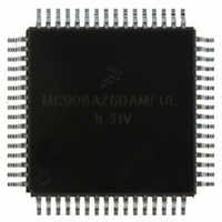
Manufacturer Part Number
MC908AZ60AMFUE
Description
IC MCU FLASH 8.4MHZ 60K 64QFP
Manufacturer
Freescale Semiconductor
Series
HC08r
Datasheet
1.MC908AZ60ACFUER.pdf
(414 pages)
Specifications of MC908AZ60AMFUE
Core Processor
HC08
Core Size
8-Bit
Speed
8.4MHz
Connectivity
CAN, SCI, SPI
Peripherals
LVD, POR, PWM
Number Of I /o
52
Program Memory Size
60KB (60K x 8)
Program Memory Type
FLASH
Eeprom Size
1K x 8
Ram Size
2K x 8
Voltage - Supply (vcc/vdd)
4.5 V ~ 5.5 V
Data Converters
A/D 15x8b
Oscillator Type
Internal
Operating Temperature
-40°C ~ 125°C
Package / Case
64-QFP
Processor Series
HC08AZ
Core
HC08
Data Bus Width
8 bit
Data Ram Size
2 KB
Interface Type
SCI, SPI
Maximum Clock Frequency
8.4 MHz
Number Of Programmable I/os
52
Number Of Timers
8
Operating Supply Voltage
5 V to 5 V
Maximum Operating Temperature
+ 125 C
Mounting Style
SMD/SMT
Development Tools By Supplier
FSICEBASE, M68CBL05CE, ZK-HC08AX-A, M68EM08AS/AZ60AE
Minimum Operating Temperature
- 40 C
On-chip Adc
8 bit, 15 Channel
Package
64PQFP
Family Name
HC08
Maximum Speed
8.4 MHz
Lead Free Status / RoHS Status
Lead free / RoHS Compliant
Available stocks
Company
Part Number
Manufacturer
Quantity
Price
Company:

Part Number:
MC908AZ60AMFUE
Manufacturer:
Freescale Semiconductor
Quantity:
135
Company:
Part Number:
MC908AZ60AMFUE
Manufacturer:
TI
Quantity:
1 433
Company:
Part Number:
MC908AZ60AMFUE
Manufacturer:
Freescale Semiconductor
Quantity:
10 000
Company:
Part Number:
MC908AZ60AMFUER
Manufacturer:
Freescale Semiconductor
Quantity:
10 000


FLASH-2 Memory
5.3 FLASH-2 Control and Block Protect Registers
The FLASH-2 array has two registers that control its operation, the FLASH-2 Control Register (FL2CR)
and the FLASH-2 Block Protect Register (FL2BPR).
5.3.1 FLASH-2 Control Register
The FLASH-2 Control Register (FL2CR) controls FLASH-2 program and erase operations.
HVEN — High-Voltage Enable Bit
MASS — Mass Erase Control Bit
ERASE — Erase Control Bit
PGM — Program Control Bit
5.3.2 FLASH-2 Block Protect Register
The FLASH-2 Block Protect Register (FL2BPR) is implemented as a byte within the FLASH-1 memory
and therefore can only be written during a FLASH programming sequence. The value in this register
determines the starting location of the protected range within the FLASH-2 memory.
62
This read/write bit enables the charge pump to drive high voltages for program and erase operations
in the array. HVEN can only be set if either PGM = 1 or ERASE = 1 and the proper sequence for
program or erase is followed.
Setting this read/write bit configures the FLASH-2 array for mass or page erase operation.
This read/write bit configures the memory for erase operation. ERASE is interlocked with the PGM bit
such that both bits cannot be set at the same time.
This read/write bit configures the memory for program operation. PGM is interlocked with the ERASE
bit such that both bits cannot be equal to 1 or set to 1 at the same time.
1 = High voltage enabled to array and charge pump on
0 = High voltage disabled to array and charge pump off
1 = Mass erase operation selected
0 = Page erase operation selected
1 = Erase operation selected
0 = Erase operation unselected
1 = Program operation selected
0 = Program operation unselected
Address:
Reset:
Read:
Write:
MC68HC908AZ60A • MC68HC908AS60A • MC68HC908AS60E Data Sheet, Rev. 6
$FE08
Bit 7
0
0
Figure 5-1. FLASH-2 Control Register (FL2CR)
= Unimplemented
6
0
0
5
0
0
4
0
0
HVEN
3
0
MASS
2
0
ERASE
1
0
Freescale Semiconductor
PGM
Bit 0
0
Related parts for MC908AZ60AMFUE
Image
Part Number
Description
Manufacturer
Datasheet
Request
R

Part Number:
Description:
Manufacturer:
Freescale Semiconductor, Inc
Datasheet:
Part Number:
Description:
Manufacturer:
Freescale Semiconductor, Inc
Datasheet:
Part Number:
Description:
Manufacturer:
Freescale Semiconductor, Inc
Datasheet:
Part Number:
Description:
Manufacturer:
Freescale Semiconductor, Inc
Datasheet:
Part Number:
Description:
Manufacturer:
Freescale Semiconductor, Inc
Datasheet:
Part Number:
Description:
Manufacturer:
Freescale Semiconductor, Inc
Datasheet:
Part Number:
Description:
Manufacturer:
Freescale Semiconductor, Inc
Datasheet:
Part Number:
Description:
Manufacturer:
Freescale Semiconductor, Inc
Datasheet:
Part Number:
Description:
Manufacturer:
Freescale Semiconductor, Inc
Datasheet:
Part Number:
Description:
Manufacturer:
Freescale Semiconductor, Inc
Datasheet:
Part Number:
Description:
Manufacturer:
Freescale Semiconductor, Inc
Datasheet:
Part Number:
Description:
Manufacturer:
Freescale Semiconductor, Inc
Datasheet:
Part Number:
Description:
Manufacturer:
Freescale Semiconductor, Inc
Datasheet:
Part Number:
Description:
Manufacturer:
Freescale Semiconductor, Inc
Datasheet:
Part Number:
Description:
Manufacturer:
Freescale Semiconductor, Inc
Datasheet: