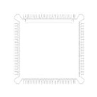
MC68332AMEH20 Freescale Semiconductor, MC68332AMEH20 Datasheet - Page 24

MC68332AMEH20
Manufacturer Part Number
MC68332AMEH20
Description
IC MCU 32BIT 20MHZ 132-PQFP
Manufacturer
Freescale Semiconductor
Series
M683xxr
Specifications of MC68332AMEH20
Core Processor
CPU32
Core Size
32-Bit
Speed
20MHz
Connectivity
EBI/EMI, SCI, SPI, UART/USART
Peripherals
POR, PWM, WDT
Number Of I /o
15
Program Memory Type
ROMless
Ram Size
2K x 8
Voltage - Supply (vcc/vdd)
4.5 V ~ 5.5 V
Oscillator Type
Internal
Operating Temperature
-40°C ~ 125°C
Package / Case
132-QFP
Processor Series
M683xx
Core
CPU32
Data Bus Width
32 bit
Controller Family/series
68K
No. Of I/o's
15
Ram Memory Size
2KB
Cpu Speed
20MHz
No. Of Timers
1
Embedded Interface Type
QSPI, SCI, UART
Digital Ic Case Style
PQFP
Rohs Compliant
Yes
Data Ram Size
2 KB
Interface Type
QSPI, SCI, UART
Maximum Clock Frequency
20 MHz
Number Of Programmable I/os
15
Number Of Timers
16
Maximum Operating Temperature
+ 125 C
Mounting Style
SMD/SMT
Minimum Operating Temperature
- 40 C
Package
132PQFP
Device Core
ColdFire
Family Name
68K/M683xx
Maximum Speed
20 MHz
Operating Supply Voltage
5 V
Lead Free Status / RoHS Status
Lead free / RoHS Compliant
Eeprom Size
-
Program Memory Size
-
Data Converters
-
Lead Free Status / Rohs Status
Lead free / RoHS Compliant
Available stocks
Company
Part Number
Manufacturer
Quantity
Price
Company:
Part Number:
MC68332AMEH20
Manufacturer:
Freescale Semiconductor
Quantity:
135
Company:
Part Number:
MC68332AMEH20
Manufacturer:
Freescale Semiconductor
Quantity:
10 000
3.3.2 Clock Synthesizer Operation
24
MOTOROLA
When an external system clock signal is applied (i.e., the PLL is not used), duty cycle of the input is
critical, especially at near maximum operating frequencies. The relationship between clock signal duty
cycle and clock signal period is expressed:
A voltage controlled oscillator (VCO) generates the system clock signal. A portion of the clock signal is
fed back to a divider/counter. The divider controls the frequency of one input to a phase comparator.
The other phase comparator input is a reference signal, either from the internal oscillator or from an
external source. The comparator generates a control signal proportional to the difference in phase be-
tween its two inputs. The signal is low-pass filtered and used to correct VCO output frequency.
The synthesizer locks when VCO frequency is identical to reference frequency. Lock time is affected by
the filter time constant and by the amount of difference between the two comparator inputs. Whenever
comparator input changes, the synthesizer must re-lock. Lock status is shown by the SLOCK bit in SYN-
CR.
The MCU does not come out of reset state until the synthesizer locks. Crystal type, characteristic fre-
quency, and layout of external oscillator circuitry affect lock time.
The low-pass filter requires an external low-leakage capacitor, typically 0.1 F, connected between the
XFC and V
V
and can be used to run the clock when the MCU is powered down. Use a quiet power supply as the
V
ternal bypass capacitors as close as possible to the V
When the clock synthesizer is used, control register SYNCR determines operating frequency and vari-
ous modes of operation. SYNCR can be read only when the processor is operating at the supervisor
privilege level.
The SYNCR X bit controls a divide by two prescaler that is not in the synthesizer feedback loop. Setting
X doubles clock speed without changing VCO speed. There is no VCO relock delay. The SYNCR W bit
controls a 3-bit prescaler in the feedback divider. Setting W increases VCO speed by a factor of four.
The SYNCR Y field determines the count modulus for a modulo 64 down counter, causing it to divide
by a value of Y
In order for the device to perform correctly, the clock frequency selected by the W, X, and Y bits must
be within the limits specified for the MCU.
The VCO frequency is twice the system clock frequency if X = 1 or four times the system clock frequency
if X = 0.
The reset state of SYNCR ($3F00) produces a modulus-64 count.
DDSYN
DDSYN
Clock frequency is determined by SYNCR bit settings as follows:
is used to power the clock circuits. A separate power source increases MCU noise immunity
source, since PLL stability depends on the VCO, which uses this supply. Place adequate ex-
DDSYN
1. When either W or Y value changes, there is a VCO relock delay.
pins.
50% — percentage variation of external clock input duty cycle
Freescale Semiconductor, Inc.
For More Information On This Product,
F
minimum external clock high/low time
SYSTEM
Minimum external clock period =
Go to: www.freescale.com
= F
REFERENCE
DDSYN
[4(Y + 1)(2
pin to ensure stable operating frequency.
2W + X
)]
MC68332TS/D
MC68332


