M30879FLFP#U3 Renesas Electronics America, M30879FLFP#U3 Datasheet - Page 81
M30879FLFP#U3
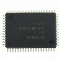
Manufacturer Part Number
M30879FLFP#U3
Description
IC M32C/87 MCU FLASH 100QFP
Manufacturer
Renesas Electronics America
Series
M16C™ M32C/80r
Datasheets
1.M3087BFLGPU3.pdf
(93 pages)
2.M3087BFLGPU3.pdf
(629 pages)
3.M3087BFLGPU3.pdf
(364 pages)
Specifications of M30879FLFP#U3
Core Processor
M32C/80
Core Size
16/32-Bit
Speed
32MHz
Connectivity
CAN, EBI/EMI, I²C, IEBus, IrDA, SIO, UART/USART
Peripherals
DMA, POR, PWM, WDT
Number Of I /o
85
Program Memory Size
1MB (1M x 8)
Program Memory Type
FLASH
Ram Size
48K x 8
Voltage - Supply (vcc/vdd)
3 V ~ 5.5 V
Data Converters
A/D 26x10b; D/A 2x8b
Oscillator Type
Internal
Operating Temperature
-40°C ~ 85°C
Package / Case
100-QFP
For Use With
R0K330879S001BE - KIT DEV RSK M32C/87R0K330879S000BE - KIT DEV RSK M32C/87
Lead Free Status / RoHS Status
Lead free / RoHS Compliant
Eeprom Size
-
Available stocks
Company
Part Number
Manufacturer
Quantity
Price


M32C/87 Group (M32C/87, M32C/87A, M32C/87B)
REJ03B0127-0151 Rev.1.51 Jul 31, 2008
Page 79 of 85
Switching Characteristics
(VCC1 = VCC2 = 3.0 to 3.6 V, VSS = 0 V, Topr = -20 to 85°C unless otherwise specified)
Table 5.53
NOTES:
td(BCLK-AD)
th(BCLK-AD)
th(RD-AD)
th(WR-AD)
td(BCLK-CS)
th(BCLK-CS)
th(RD-CS)
th(WR-CS)
td(BCLK-RD)
th(BCLK-RD)
td(BCLK-WR)
th(BCLK-WR)
td(DB-WR)
th(WR-DB)
td(BCLK-ALE)
th(BCLK-ALE)
td(AD-ALE)
th(ALE-AD)
tdz(RD-AD)
1. Values, which depend on BCLK frequency, can be obtained from the following equations.
2. Values, which depend on BCLK frequency and external bus cycles, can be obtained from the following equation.
3. Values, which depend on BCLK frequency and external bus cycles, can be obtained from the following equation.
4. Values, which depend on BCLK frequency and external bus cycles, can be obtained from the following equation.
5. tc [ns] is added when recovery cycle is inserted.
Symbol
th(WR-DB) =
th(RD-AD)
th(WR-AD) =
th(RD-CS)
th(WR-CS) =
td(DB-WR) =
td(AD-ALE) =
th(ALE-AD) =
Memory Expansion Mode and Microprocessor Mode (when accessing external
memory space with multiplexed bus)
Address output delay time
Address output hold time (BCLK standard)
Address output hold time (RD standard)
Address output hold time (WR standard)
Chip-select signal output delay time
Chip-select signal output hold time (BCLK standard)
Chip-select signal output hold time (RD standard)
Chip-select signal output hold time (WR standard)
RD signal output delay time
RD signal output hold time
WR signal output delay time
WR signal output hold time
Data output delay time (WR standard)
Data output hold time (WR standard)
ALE signal output delay time (BCLK standard)
ALE signal output hold time (BCLK standard)
ALE signal output delay time (address standard)
ALE signal output hold time (address standard)
Address output float start time
=
=
f(BCLK) × 2
f(BCLK) × 2
f(BCLK) × 2
f(BCLK) × 2
f(BCLK) × 2
f(BCLK) × 2
f(BCLK) × 2
f(BCLK) × 2
10
10
10
9
9
9
10
10
10
10
10
× m
× n
× n
9
9
9
9
9
- 20 [ns]
- 10 [ns]
- 15 [ns]
- 10 [ns]
- 10 [ns]
- 25 [ns] (if external bus cycle is a φ + b φ , m = (b × 2) - 1)
- 20 [ns] (if external bus cycle is a φ + b φ , n = a)
- 20 [ns] (if external bus cycle is a φ + b φ , n = a)
Parameter
(5)
(5)
(5)
(5)
(5)
See Figure 5.2
Measurement
Condition
VCC1 = VCC2 = 3.3 V
5. Electrical Characteristics
(note 1)
(note 1)
(note 1)
(note 1)
(note 2)
(note 1)
(note 3)
(note 4)
Min.
-3
-3
-5
-2
0
Standard
Max.
18
18
18
18
18
8
Unit
ns
ns
ns
ns
ns
ns
ns
ns
ns
ns
ns
ns
ns
ns
ns
ns
ns
ns
ns
Related parts for M30879FLFP#U3
Image
Part Number
Description
Manufacturer
Datasheet
Request
R

Part Number:
Description:
KIT STARTER FOR M16C/29
Manufacturer:
Renesas Electronics America
Datasheet:

Part Number:
Description:
KIT STARTER FOR R8C/2D
Manufacturer:
Renesas Electronics America
Datasheet:

Part Number:
Description:
R0K33062P STARTER KIT
Manufacturer:
Renesas Electronics America
Datasheet:

Part Number:
Description:
KIT STARTER FOR R8C/23 E8A
Manufacturer:
Renesas Electronics America
Datasheet:

Part Number:
Description:
KIT STARTER FOR R8C/25
Manufacturer:
Renesas Electronics America
Datasheet:

Part Number:
Description:
KIT STARTER H8S2456 SHARPE DSPLY
Manufacturer:
Renesas Electronics America
Datasheet:

Part Number:
Description:
KIT STARTER FOR R8C38C
Manufacturer:
Renesas Electronics America
Datasheet:

Part Number:
Description:
KIT STARTER FOR R8C35C
Manufacturer:
Renesas Electronics America
Datasheet:

Part Number:
Description:
KIT STARTER FOR R8CL3AC+LCD APPS
Manufacturer:
Renesas Electronics America
Datasheet:
Part Number:
Description:
KIT STARTER FOR RX610
Manufacturer:
Renesas Electronics America
Datasheet:

Part Number:
Description:
KIT STARTER FOR R32C/118
Manufacturer:
Renesas Electronics America
Datasheet:

Part Number:
Description:
KIT DEV RSK-R8C/26-29
Manufacturer:
Renesas Electronics America
Datasheet:

Part Number:
Description:
KIT STARTER FOR SH7124
Manufacturer:
Renesas Electronics America
Datasheet:

Part Number:
Description:
KIT STARTER FOR H8SX/1622
Manufacturer:
Renesas Electronics America
Datasheet:

Part Number:
Description:
KIT DEV FOR SH7203
Manufacturer:
Renesas Electronics America
Datasheet: