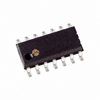
PIC16F526-E/SL Microchip Technology, PIC16F526-E/SL Datasheet - Page 87

PIC16F526-E/SL
Manufacturer Part Number
PIC16F526-E/SL
Description
IC PIC MCU FLASH 1KX12 14SOIC
Manufacturer
Microchip Technology
Series
PIC® 16Fr
Specifications of PIC16F526-E/SL
Core Size
8-Bit
Program Memory Size
1.5KB (1K x 12)
Core Processor
PIC
Speed
20MHz
Peripherals
POR, WDT
Number Of I /o
11
Program Memory Type
FLASH
Ram Size
67 x 8
Voltage - Supply (vcc/vdd)
2 V ~ 5.5 V
Data Converters
A/D 3x8b
Oscillator Type
Internal
Operating Temperature
-40°C ~ 125°C
Package / Case
14-SOIC (3.9mm Width), 14-SOL
Controller Family/series
PIC16F
No. Of I/o's
12
Eeprom Memory Size
64Byte
Ram Memory Size
67Byte
Cpu Speed
20MHz
No. Of Timers
1
Lead Free Status / RoHS Status
Lead free / RoHS Compliant
For Use With
ICE2000 - EMULATOR MPLAB-ICE 2000 POD
Eeprom Size
-
Connectivity
-
Lead Free Status / RoHS Status
Lead free / RoHS Compliant, Lead free / RoHS Compliant
TABLE 14-1:
2010 Microchip Technology Inc.
DC CHARACTERISTICS
Param
D030
D030A
D031
D032
D033
D033
D033
D040
D040A
D041
D042
D042A
D042A
D043
D070
D060
D061
D063
D080
D080A
D090
D090A
D100
D101
D120
D120A E
D121
Note 1: In EXTRC oscillator configuration, the OSC1/CLKIN pin is a Schmitt Trigger input. It is not recommended that the
No.
†
2: Negative current is defined as coming out of the pin.
3: This spec. applies to RB3/MCLR configured as RB3 with pull-up disabled.
4: This spec. applies to all weak pull-up devices, including the weak pull-up found on RB3/MCLR. The current value listed
5: The leakage current on the nMCLR pin is strongly dependent on the applied voltage level. The specified levels represent
V
COSC2 OSC2 pin
CIO
E
V
Sym.
I
V
V
PUR
V
OH
D
D
DRW
I
IL
OL
Data in “Typ” column is at 5V, 25C unless otherwise stated. These parameters are for design guidance only and are not tested.
PIC16F526 be driven with external clock in RC mode.
will be the same whether or not the pin is configured as RB3 with pull-up enabled or as MCLR.
normal operating conditions. Higher leakage may be measured at different input voltages.
IH
IL
Input Low Voltage
I/O ports
with TTL buffer
with Schmitt Trigger buffer
MCLR, T0CKI
OSC1 (EXTRC mode), EC
OSC1 (HS mode)
OSC1 (XT and LP modes)
Input High Voltage
I/O ports
with TTL buffer
with Schmitt Trigger buffer
MCLR, T0CKI
OSC1 (EXTRC mode), EC
OSC1 (HS mode)
OSC1 (XT and LP modes)
PORTB weak pull-up current
Input Leakage Current
I/O ports
RB3/MCLR
OSC1
Output Low Voltage
I/O ports/CLKOUT
Output High Voltage
I/O ports/CLKOUT
Capacitive Loading Specs on Output Pins
All I/O pins and OSC2
Flash Data Memory
Byte endurance
Byte endurance
V
DD
for read/write
DC CHARACTERISTICS: PIC16F526 (Industrial, Extended)
Characteristic
(3)
(2,5)
(1)
(1)
(4)
Standard Operating Conditions (unless otherwise specified)
Operating temperature
Operating voltage V
V
V
0.25V
0.85V
0.85V
0.85V
0.7V
DD
DD
+ 0.8V
100K
Min.
V
Vss
Vss
Vss
Vss
Vss
Vss
Vss
10K
2.0
1.6
50
—
—
—
—
—
—
—
MIN
– 0.7
– 0.7
DD
DD
DD
DD
DD
Typ.†
100K
±0.7
250
1M
—
—
—
—
—
—
—
—
—
—
—
—
—
—
—
—
—
—
—
—
—
—
—
—
DD
0.15 V
0.15 V
0.15 V
0.15 V
0.3 V
Max.
V
V
V
V
V
V
V
400
range as described in DC spec.
0.8
0.3
0.6
0.6
5.5
±1
±5
±5
—
—
15
50
—
—
DD
DD
DD
DD
DD
DD
DD
DD
DD
DD
DD
DD
-40°C T
-40°C T
Units
E/W
E/W
A
A
A
A
pF
pF
V
V
V
V
V
V
V
V
V
V
V
V
V
V
V
V
V
V
V
A
A
For all 4.5 V
Otherwise
4.5 V
Otherwise
For entire V
V
Vss V
Vss V
Vss V
configuration
I
I
I
I
In XT, HS and LP modes when external clock is
used to drive OSC1.
–40C T
+85C T
OL
OL
OH
OH
+85°C (industrial)
+125°C (extended)
DD
= 8.5 mA, V
= 7.0 mA, V
= -3.0 mA, V
= -2.5 mA, V
= 5V, V
DD
PIN
PIN
PIN
A
A
5.5V
V
V
V
+85C
+125C
DD
PIN
PIC16F526
DD
DD
DD
DD
range
DD
DD
= V
DD
DD
5.5V
, Pin at high-impedance
, XT, HS and LP osc
Conditions
= 4.5V, –40C to +85C
= 4.5V, –40C to +125C
SS
= 4.5V, –40C to +85C
= 4.5V, –40C to +125C
DS41326E-page 87


