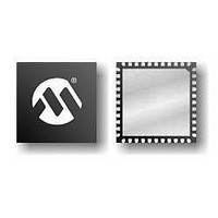
PIC18F47J53T-I/ML Microchip Technology, PIC18F47J53T-I/ML Datasheet - Page 370

PIC18F47J53T-I/ML
Manufacturer Part Number
PIC18F47J53T-I/ML
Description
IC MCU 8BIT 128KB FLASH 44 QFN
Manufacturer
Microchip Technology
Series
PIC® XLP™ 18Fr
Specifications of PIC18F47J53T-I/ML
Program Memory Type
FLASH
Program Memory Size
128KB (64K x 16)
Package / Case
*
Core Processor
PIC
Core Size
8-Bit
Speed
48MHz
Connectivity
I²C, LIN, SPI, UART/USART, USB
Peripherals
Brown-out Detect/Reset, POR, PWM, WDT
Number Of I /o
34
Ram Size
3.8K x 8
Voltage - Supply (vcc/vdd)
2.15 V ~ 3.6 V
Data Converters
A/D 13x10b/12b
Oscillator Type
Internal
Operating Temperature
-40°C ~ 85°C
Processor Series
PIC18F
Core
PIC
Data Bus Width
8 bit
Data Ram Size
3.8 KB
Interface Type
I2C, SPI, USART
Maximum Clock Frequency
48 MHz
Number Of Programmable I/os
22
Number Of Timers
8
Operating Supply Voltage
2.15 V to 3.6 V
Maximum Operating Temperature
+ 85 C
Mounting Style
SMD/SMT
3rd Party Development Tools
52715-96, 52716-328, 52717-734, 52712-325, EWPIC18
Minimum Operating Temperature
- 40 C
Lead Free Status / RoHS Status
Lead free / RoHS Compliant
For Use With
MA180029 - BOARD DEMO PIC18F47J53 FS USB
Eeprom Size
-
Lead Free Status / Rohs Status
Lead free / RoHS Compliant
Available stocks
Company
Part Number
Manufacturer
Quantity
Price
Company:
Part Number:
PIC18F47J53T-I/ML
Manufacturer:
MURATA
Quantity:
640 000
- Current page: 370 of 586
- Download datasheet (6Mb)
PIC18F47J53 FAMILY
REGISTER 22-3:
DS39964B-page 370
bit 7
Legend:
R = Readable bit
-n = Value at POR
bit 7-4
bit 3
bit 2
bit 1
bit 0
U-1
—
Unimplemented: Program the corresponding Flash Configuration bit to ‘1’
MSSPMSK: MSSP 7-Bit Address Masking Mode Enable bit
1 = 7-Bit Address Masking mode enabled
0 = 5-Bit Address Masking mode enabled
Unimplemented: Read as ‘0’
ADCSEL: A/D Converter Mode bit
1 = 10-Bit Conversion mode enabled
0 = 12-Bit Conversion mode enabled
IOL1WAY: IOLOCK One Way Set Enable bit
1 = IOLOCK bit (PPSCON<0>) can be set once, provided the unlock sequence has been completed.
0 = IOLOCK bit (PPSCON<0>) can be set and cleared as needed, provided the unlock sequence has
Once set, the Peripheral Pin Select registers cannot be written to a second time.
been completed
U-1
—
CONFIG3H: CONFIGURATION REGISTER 3 HIGH (BYTE ADDRESS 300005h)
WO = Write-Once bit
‘1’ = Bit is set
U-1
—
U-1
Preliminary
—
U = Unimplemented bit, read as ‘0’
‘0’ = Bit is cleared
MSSPMSK
R/WO-1
U-0
—
2010 Microchip Technology Inc.
x = Bit is unknown
ADCSEL
R/WO-1
IOL1WAY
R/WO-1
bit 0
Related parts for PIC18F47J53T-I/ML
Image
Part Number
Description
Manufacturer
Datasheet
Request
R

Part Number:
Description:
Manufacturer:
Microchip Technology Inc.
Datasheet:

Part Number:
Description:
Manufacturer:
Microchip Technology Inc.
Datasheet:

Part Number:
Description:
Manufacturer:
Microchip Technology Inc.
Datasheet:

Part Number:
Description:
Manufacturer:
Microchip Technology Inc.
Datasheet:

Part Number:
Description:
Manufacturer:
Microchip Technology Inc.
Datasheet:

Part Number:
Description:
Manufacturer:
Microchip Technology Inc.
Datasheet:

Part Number:
Description:
Manufacturer:
Microchip Technology Inc.
Datasheet:

Part Number:
Description:
Manufacturer:
Microchip Technology Inc.
Datasheet:


