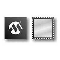
PIC18F47J53T-I/ML Microchip Technology, PIC18F47J53T-I/ML Datasheet - Page 40

PIC18F47J53T-I/ML
Manufacturer Part Number
PIC18F47J53T-I/ML
Description
IC MCU 8BIT 128KB FLASH 44 QFN
Manufacturer
Microchip Technology
Series
PIC® XLP™ 18Fr
Specifications of PIC18F47J53T-I/ML
Program Memory Type
FLASH
Program Memory Size
128KB (64K x 16)
Package / Case
*
Core Processor
PIC
Core Size
8-Bit
Speed
48MHz
Connectivity
I²C, LIN, SPI, UART/USART, USB
Peripherals
Brown-out Detect/Reset, POR, PWM, WDT
Number Of I /o
34
Ram Size
3.8K x 8
Voltage - Supply (vcc/vdd)
2.15 V ~ 3.6 V
Data Converters
A/D 13x10b/12b
Oscillator Type
Internal
Operating Temperature
-40°C ~ 85°C
Processor Series
PIC18F
Core
PIC
Data Bus Width
8 bit
Data Ram Size
3.8 KB
Interface Type
I2C, SPI, USART
Maximum Clock Frequency
48 MHz
Number Of Programmable I/os
22
Number Of Timers
8
Operating Supply Voltage
2.15 V to 3.6 V
Maximum Operating Temperature
+ 85 C
Mounting Style
SMD/SMT
3rd Party Development Tools
52715-96, 52716-328, 52717-734, 52712-325, EWPIC18
Minimum Operating Temperature
- 40 C
Lead Free Status / RoHS Status
Lead free / RoHS Compliant
For Use With
MA180029 - BOARD DEMO PIC18F47J53 FS USB
Eeprom Size
-
Lead Free Status / Rohs Status
Lead free / RoHS Compliant
Available stocks
Company
Part Number
Manufacturer
Quantity
Price
Company:
Part Number:
PIC18F47J53T-I/ML
Manufacturer:
MURATA
Quantity:
640 000
- Current page: 40 of 586
- Download datasheet (6Mb)
PIC18F47J53 FAMILY
REGISTER 3-1:
3.3
When the PIC18F47J53 family devices are used for
USB connectivity, a 6 MHz or 48 MHz clock must be
provided to the USB module for operation in either
Low-Speed or Full-Speed modes, respectively. This
may require some forethought in selecting an oscillator
frequency and programming the device.
The full range of possible oscillator configurations
compatible with USB operation is shown in Table 3-5.
TABLE 3-4:
DS39964B-page 40
bit 7
Legend:
R = Readable bit
-n = Value at POR
bit 7
bit 6
bit 5-0
Note 1:
System Clock
INTSRC
R/W-0
48
48
48
48
24
24
24
24
Oscillator Settings for USB
When the CFGPLLEN Configuration bit is used to enable the PLL, clearing OSCTUNE<6> will not disable
the PLL.
INTSRC: Internal Oscillator Low-Frequency Source Select bit
1 = 31.25 kHz device clock derived from 8 MHz INTOSC source (divide-by-256 enabled)
0 = 31 kHz device clock derived directly from INTRC internal oscillator
PLLEN: Frequency Multiplier Enable bit
1 = 96 MHz PLL is enabled
0 = 96 MHz PLL is disabled
TUN<5:0>: Frequency Tuning bits
011111 = Maximum frequency
011110
•
•
•
000001
000000 = Center frequency; oscillator module is running at the calibrated frequency
111111
•
•
•
100000 = Minimum frequency
CLOCK FOR LOW-SPEED USB
PLLEN
R/W-0
CPDIV<1:0>
OSCTUNE: OSCILLATOR TUNING REGISTER (ACCESS F9Bh)
(1)
11
10
01
00
11
10
01
00
W = Writable bit
‘1’ = Bit is set
R/W-0
TUN5
Microcontroller Clock
48/2 = 24 MHz
48/3 = 16 MHz
24/2 = 12 MHz
48/6 = 8 MHz
24/3 = 8 MHz
24/6 = 4 MHz
R/W-0
TUN4
48 MHz
24 MHz
Preliminary
(1)
U = Unimplemented bit, read as ‘0’
‘0’ = Bit is cleared
R/W-0
TUN3
3.3.1
The USB clock for Low-Speed mode is derived from the
primary oscillator or from the 96 MHz PLL. In order to
operate the USB module in Low-Speed mode, a 6 MHz
clock must be provided to the USB module.
See Table 3-4 and Table 3-5 for possible combinations
which can be used for low-speed USB operation.
LS48MHZ
LOW-SPEED OPERATION
R/W-0
TUN2
1
1
1
1
0
0
0
0
2010 Microchip Technology Inc.
x = Bit is unknown
R/W-0
TUN1
48/8 = 6 MHz
48/8 = 6 MHz
48/8 = 6 MHz
48/8 = 6 MHz
24/4 = 6 MHz
24/4 = 6 MHz
24/4 = 6 MHz
24/4 = 6 MHz
USB Clock
R/W-0
TUN0
bit 0
Related parts for PIC18F47J53T-I/ML
Image
Part Number
Description
Manufacturer
Datasheet
Request
R

Part Number:
Description:
Manufacturer:
Microchip Technology Inc.
Datasheet:

Part Number:
Description:
Manufacturer:
Microchip Technology Inc.
Datasheet:

Part Number:
Description:
Manufacturer:
Microchip Technology Inc.
Datasheet:

Part Number:
Description:
Manufacturer:
Microchip Technology Inc.
Datasheet:

Part Number:
Description:
Manufacturer:
Microchip Technology Inc.
Datasheet:

Part Number:
Description:
Manufacturer:
Microchip Technology Inc.
Datasheet:

Part Number:
Description:
Manufacturer:
Microchip Technology Inc.
Datasheet:

Part Number:
Description:
Manufacturer:
Microchip Technology Inc.
Datasheet:


