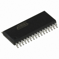
AT90PWM316-16SU Atmel, AT90PWM316-16SU Datasheet - Page 203

AT90PWM316-16SU
Manufacturer Part Number
AT90PWM316-16SU
Description
MCU AVR 16K ISP FLSH 16MHZ32SOIC
Manufacturer
Atmel
Series
AVR® 90PWM Lightingr
Datasheet
1.AT90PWM216-16SU.pdf
(359 pages)
Specifications of AT90PWM316-16SU
Core Processor
AVR
Core Size
8-Bit
Speed
16MHz
Connectivity
SPI, UART/USART
Peripherals
Brown-out Detect/Reset, POR, PWM, WDT
Number Of I /o
27
Program Memory Size
16KB (16K x 8)
Program Memory Type
FLASH
Eeprom Size
512 x 8
Ram Size
1K x 8
Voltage - Supply (vcc/vdd)
2.7 V ~ 5.5 V
Data Converters
A/D 11x10b; D/A 1x10b
Oscillator Type
Internal
Operating Temperature
-40°C ~ 105°C
Package / Case
32-SOIC (7.5mm Width)
Processor Series
AT90PWMx
Core
AVR8
Data Bus Width
8 bit
Data Ram Size
1 KB
Interface Type
SPI, UART
Maximum Clock Frequency
16 MHz
Number Of Programmable I/os
53
Number Of Timers
2
Operating Supply Voltage
2.7 V to 5.5 V
Maximum Operating Temperature
+ 105 C
Mounting Style
SMD/SMT
3rd Party Development Tools
EWAVR, EWAVR-BL
Development Tools By Supplier
ATAVRDRAGON, ATSTK500, ATSTK600, ATAVRISP2, ATAVRONEKIT, ATAVRFBKIT, ATAVRISP2
Minimum Operating Temperature
- 40 C
On-chip Adc
10 bit, 11 Channel
Package
32SOIC
Device Core
AVR
Family Name
90P
Maximum Speed
16 MHz
For Use With
ATSTK600-SOIC - STK600 SOCKET/ADAPTER FOR SOIC770-1007 - ISP 4PORT ATMEL AVR MCU SPI/JTAG770-1005 - ISP 4PORT FOR ATMEL AVR MCU JTAG770-1004 - ISP 4PORT FOR ATMEL AVR MCU SPIATAVRMC200 - KIT EVAL FOR AT90PWM3 ASYNCATAVRFBKIT - KIT DEMO BALLAST FOR AT90PWM2ATAVRISP2 - PROGRAMMER AVR IN SYSTEM
Lead Free Status / RoHS Status
Lead free / RoHS Compliant
Available stocks
Company
Part Number
Manufacturer
Quantity
Price
Part Number:
AT90PWM316-16SU
Manufacturer:
ATMEL/爱特梅尔
Quantity:
20 000
- Current page: 203 of 359
- Download datasheet (6Mb)
18.9.2
18.10 USART Register Description
18.10.1
7710E–AVR–08/10
Using MPCM
USART I/O Data Register – UDR
For an MCU to act as a master MCU, it can use a 9-bit character frame format (UCSZ = 7). The
ninth bit (TXB8) must be set when an address frame (TXB8 = 1) or cleared when a data frame
(TXBn = 0) is being transmitted. The slave MCUs must in this case be set to use a 9-bit charac-
ter frame format.
The following procedure should be used to exchange data in Multi-processor Communication
mode:
Using any of the 5- to 8-bit character frame formats is possible, but impractical since the
Receiver must change between using N and N+1 character frame formats. This makes full-
duplex operation difficult since the Transmitter and Receiver use the same character size set-
ting. If 5- to 8-bit character frames are used, the Transmitter must be set to use two stop bit
(USBS = 1) since the first stop bit is used for indicating the frame type.
• Bit 7:0 – RxB7:0: Receive Data Buffer (read access)
• Bit 7:0 – TxB7:0: Transmit Data Buffer (write access)
The USART Transmit Data Buffer Register and USART Receive Data Buffer Registers share the
same I/O address referred to as USART Data Register or UDR. The Transmit Data Buffer Reg-
ister (TXBn) will be the destination for data written to the UDR Register location. Reading the
UDR Register location will return the contents of the Receive Data Buffer Register (RXBn).
For 5-, 6-, or 7-bit characters the upper unused bits will be ignored by the Transmitter and set to
zero by the Receiver.
The transmit buffer can only be written when the UDRE flag in the UCSRA Register is set. Data
written to UDR when the UDRE flag is not set, will be ignored by the USART Transmitter. When
data is written to the transmit buffer, and the Transmitter is enabled, the Transmitter will load the
data into the Transmit Shift Register when the Shift Register is empty. Then the data will be seri-
ally transmitted on the TxDn pin.
1. All Slave MCUs are in Multi-processor Communication mode (MPCM in
2. The Master MCU sends an address frame, and all slaves receive and read this frame.
3. Each Slave MCU reads the UDR Register and determines if it has been selected. If so,
4. The addressed MCU will receive all data frames until a new address frame is received.
5. When the last data frame is received by the addressed MCU, the addressed MCU sets
Initial Value
Read/Write
UCSRA is set).
In the Slave MCUs, the RXC flag in UCSRA will be set as normal.
it clears the MPCM bit in UCSRA, otherwise it waits for the next address byte and
keeps the MPCM setting.
The other Slave MCUs, which still have the MPCM bit set, will ignore the data frames.
the MPCM bit and waits for a new address frame from master. The process then
repeats from 2.
Bit
R/W
7
0
R/W
6
0
R/W
5
0
R/W
4
0
RXB[7:0]
TXB[7:0]
R/W
3
0
R/W
2
0
AT90PWM216/316
R/W
1
0
R/W
0
0
UDR (Write)
UDR (Read)
203
Related parts for AT90PWM316-16SU
Image
Part Number
Description
Manufacturer
Datasheet
Request
R

Part Number:
Description:
IC AVR MCU FLASH 8K 32QFN
Manufacturer:
Atmel
Datasheet:

Part Number:
Description:
IC AVR MCU FLASH 8K 32SOIC
Manufacturer:
Atmel
Datasheet:

Part Number:
Description:
MCU AVR 8K FLASH 16MHZ 32-QFN
Manufacturer:
Atmel
Datasheet:

Part Number:
Description:
DEV KIT FOR AVR/AVR32
Manufacturer:
Atmel
Datasheet:

Part Number:
Description:
INTERVAL AND WIPE/WASH WIPER CONTROL IC WITH DELAY
Manufacturer:
ATMEL Corporation
Datasheet:

Part Number:
Description:
Low-Voltage Voice-Switched IC for Hands-Free Operation
Manufacturer:
ATMEL Corporation
Datasheet:

Part Number:
Description:
MONOLITHIC INTEGRATED FEATUREPHONE CIRCUIT
Manufacturer:
ATMEL Corporation
Datasheet:

Part Number:
Description:
AM-FM Receiver IC U4255BM-M
Manufacturer:
ATMEL Corporation
Datasheet:

Part Number:
Description:
Monolithic Integrated Feature Phone Circuit
Manufacturer:
ATMEL Corporation
Datasheet:

Part Number:
Description:
Multistandard Video-IF and Quasi Parallel Sound Processing
Manufacturer:
ATMEL Corporation
Datasheet:

Part Number:
Description:
High-performance EE PLD
Manufacturer:
ATMEL Corporation
Datasheet:

Part Number:
Description:
8-bit Flash Microcontroller
Manufacturer:
ATMEL Corporation
Datasheet:


