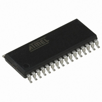
AT90PWM316-16SU Atmel, AT90PWM316-16SU Datasheet - Page 95

AT90PWM316-16SU
Manufacturer Part Number
AT90PWM316-16SU
Description
MCU AVR 16K ISP FLSH 16MHZ32SOIC
Manufacturer
Atmel
Series
AVR® 90PWM Lightingr
Datasheet
1.AT90PWM216-16SU.pdf
(359 pages)
Specifications of AT90PWM316-16SU
Core Processor
AVR
Core Size
8-Bit
Speed
16MHz
Connectivity
SPI, UART/USART
Peripherals
Brown-out Detect/Reset, POR, PWM, WDT
Number Of I /o
27
Program Memory Size
16KB (16K x 8)
Program Memory Type
FLASH
Eeprom Size
512 x 8
Ram Size
1K x 8
Voltage - Supply (vcc/vdd)
2.7 V ~ 5.5 V
Data Converters
A/D 11x10b; D/A 1x10b
Oscillator Type
Internal
Operating Temperature
-40°C ~ 105°C
Package / Case
32-SOIC (7.5mm Width)
Processor Series
AT90PWMx
Core
AVR8
Data Bus Width
8 bit
Data Ram Size
1 KB
Interface Type
SPI, UART
Maximum Clock Frequency
16 MHz
Number Of Programmable I/os
53
Number Of Timers
2
Operating Supply Voltage
2.7 V to 5.5 V
Maximum Operating Temperature
+ 105 C
Mounting Style
SMD/SMT
3rd Party Development Tools
EWAVR, EWAVR-BL
Development Tools By Supplier
ATAVRDRAGON, ATSTK500, ATSTK600, ATAVRISP2, ATAVRONEKIT, ATAVRFBKIT, ATAVRISP2
Minimum Operating Temperature
- 40 C
On-chip Adc
10 bit, 11 Channel
Package
32SOIC
Device Core
AVR
Family Name
90P
Maximum Speed
16 MHz
For Use With
ATSTK600-SOIC - STK600 SOCKET/ADAPTER FOR SOIC770-1007 - ISP 4PORT ATMEL AVR MCU SPI/JTAG770-1005 - ISP 4PORT FOR ATMEL AVR MCU JTAG770-1004 - ISP 4PORT FOR ATMEL AVR MCU SPIATAVRMC200 - KIT EVAL FOR AT90PWM3 ASYNCATAVRFBKIT - KIT DEMO BALLAST FOR AT90PWM2ATAVRISP2 - PROGRAMMER AVR IN SYSTEM
Lead Free Status / RoHS Status
Lead free / RoHS Compliant
Available stocks
Company
Part Number
Manufacturer
Quantity
Price
Part Number:
AT90PWM316-16SU
Manufacturer:
ATMEL/爱特梅尔
Quantity:
20 000
- Current page: 95 of 359
- Download datasheet (6Mb)
14.7
7710E–AVR–08/10
Timer/Counter Timing Diagrams
one allows the OC0A pin to toggle on Compare Matches if the WGM02 bit is set. This option is
not available for the OC0B pin (see
visible on the port pin if the data direction for the port pin is set as output. The PWM waveform is
generated by clearing (or setting) the OC0x Register at the compare match between OCR0x and
TCNT0 when the counter increments, and setting (or clearing) the OC0x Register at compare
match between OCR0x and TCNT0 when the counter decrements. The PWM frequency for the
output when using phase correct PWM can be calculated by the following equation:
The N variable represents the prescale factor (1, 8, 64, 256, or 1024).
The extreme values for the OCR0A Register represent special cases when generating a PWM
waveform output in the phase correct PWM mode. If the OCR0A is set equal to BOTTOM, the
output will be continuously low and if set equal to MAX the output will be continuously high for
non-inverted PWM mode. For inverted PWM the output will have the opposite logic values.
At the very start of period 2 in
there is no Compare Match. The point of this transition is to guarantee symmetry around BOT-
TOM. There are two cases that give a transition without Compare Match.
The Timer/Counter is a synchronous design and the timer clock (clk
clock enable signal in the following figures. The figures include information on when interrupt
flags are set.
shows the count sequence close to the MAX value in all modes other than phase correct PWM
mode.
Figure 14-8. Timer/Counter Timing Diagram, no Prescaling
Figure 14-9
• OCRnx changes its value from MAX, like in
• The timer starts counting from a value higher than the one in OCRnx, and for that reason
OCn pin value is the same as the result of a down-counting Compare Match. To ensure
symmetry around BOTTOM the OCnx value at MAX must correspond to the result of an up-
counting Compare Match.
misses the Compare Match and hence the OCnx change that would have happened on the
way up.
TCNTn
(clk
TOVn
clk
clk
I/O
I/O
Tn
/1)
shows the same timing data, but with the prescaler enabled.
Figure 14-8
MAX - 1
contains timing data for basic Timer/Counter operation. The figure
Figure 14-7
Table 14-7 on page
f
OCnxPCPWM
OCnx has a transition from high to low even though
MAX
Figure
=
----------------- -
N 510
f
clk_I/O
14-7. When the OCR0A value is MAX the
⋅
99). The actual OC0x value will only be
AT90PWM216/316
BOTTOM
T0
) is therefore shown as a
BOTTOM + 1
95
Related parts for AT90PWM316-16SU
Image
Part Number
Description
Manufacturer
Datasheet
Request
R

Part Number:
Description:
IC AVR MCU FLASH 8K 32QFN
Manufacturer:
Atmel
Datasheet:

Part Number:
Description:
IC AVR MCU FLASH 8K 32SOIC
Manufacturer:
Atmel
Datasheet:

Part Number:
Description:
MCU AVR 8K FLASH 16MHZ 32-QFN
Manufacturer:
Atmel
Datasheet:

Part Number:
Description:
DEV KIT FOR AVR/AVR32
Manufacturer:
Atmel
Datasheet:

Part Number:
Description:
INTERVAL AND WIPE/WASH WIPER CONTROL IC WITH DELAY
Manufacturer:
ATMEL Corporation
Datasheet:

Part Number:
Description:
Low-Voltage Voice-Switched IC for Hands-Free Operation
Manufacturer:
ATMEL Corporation
Datasheet:

Part Number:
Description:
MONOLITHIC INTEGRATED FEATUREPHONE CIRCUIT
Manufacturer:
ATMEL Corporation
Datasheet:

Part Number:
Description:
AM-FM Receiver IC U4255BM-M
Manufacturer:
ATMEL Corporation
Datasheet:

Part Number:
Description:
Monolithic Integrated Feature Phone Circuit
Manufacturer:
ATMEL Corporation
Datasheet:

Part Number:
Description:
Multistandard Video-IF and Quasi Parallel Sound Processing
Manufacturer:
ATMEL Corporation
Datasheet:

Part Number:
Description:
High-performance EE PLD
Manufacturer:
ATMEL Corporation
Datasheet:

Part Number:
Description:
8-bit Flash Microcontroller
Manufacturer:
ATMEL Corporation
Datasheet:


