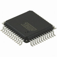
AT32UC3L064-AUR Atmel, AT32UC3L064-AUR Datasheet - Page 60

AT32UC3L064-AUR
Manufacturer Part Number
AT32UC3L064-AUR
Description
IC MCU AVR32 64K FLASH 48TQFP
Manufacturer
Atmel
Series
AVR®32 UC3r
Datasheet
1.AT32UC3L016-ZAUR.pdf
(71 pages)
Specifications of AT32UC3L064-AUR
Package / Case
48-TQFP, 48-VQFP
Voltage - Supply (vcc/vdd)
1.62 V ~ 1.98 V
Operating Temperature
-40°C ~ 85°C
Speed
50MHz
Number Of I /o
36
Core Processor
AVR
Program Memory Type
FLASH
Ram Size
16K x 8
Program Memory Size
64KB (64K x 8)
Data Converters
A/D 9x10b
Oscillator Type
Internal
Peripherals
Brown-out Detect/Reset, DMA, PWM, WDT
Connectivity
I²C, SPI, UART/USART
Core Size
32-Bit
Lead Free Status / RoHS Status
Lead free / RoHS Compliant
Eeprom Size
-
Available stocks
Company
Part Number
Manufacturer
Quantity
Price
Company:
Part Number:
AT32UC3L064-AUR
Manufacturer:
ATMEL
Quantity:
101
32099AS–AVR32–06/09
2. The DFLL should be slowed down before disabled
3. Writing to SCIF ICR masks new interrupts received in the same clock cycle
4. FINE value for DFLL is not correct when dithering is disabled
5. BODVERSION register reads 0x100
7. BRIFA is non-functional
8. VREGCR DEEPMODEDISABLE bit is not readable
9. DFLL step size should be 7 or lower below 30 MHz
10. Generic clock sources are kept running in sleep modes
A Supply Monitor 33 reset will not be detected in the Reset Cause register (RCAUSE) as
BOD33, it will be detected as a Power-on Reset (POR).
Fix/Workaround
None.
The frequency of the DFLL should be set to minimum before disabled.
Fix/Workaround
Before disabling the DFLL the value of the COARSE register should be set to
zero.
Writing to SCIF ICR masks any new SCIF interrupt received in the same clock
cycle, regardless of write value.
Fix/Workaround:
For every interrupt except BODDET, SM33DET, and VREGOK the CLKSR register can be
read to detect new interrupts. BODDET, SM33DET and VREGOK interrupts will not be gen-
erated if they occur when writing SCIF ICR.
In open loop mode, the FINE value used by the DFLL DAC is offseted by two compared to
the value written to the DFLL0CONF.FINE field. I. e. the value to the DFLL DAC is
DFLL0CONF.FINE-0x002. If DFLL0CONF.FINE is written to 0x000, 0x001 or 0x002 the
value to the DFLL DAC will be 0x1FE, 0x1FF or 0x000 respectively.
Fix/workaround
Write the desired value added by two to the DFLL0CONF.FINE field.
The BODVERSION register reads 0x100 instead of 0x101.
Fix/Workaround
None.
BRIFA is non-functional.
Fix/Workaround
None.
VREGCR DEEPMODEDISABLE bit is not readable.
Fix/workaround
None.
If max step size is above 7, the DFLL might not lock at the correct frequency if the target fre-
quency is below 30 MHz.
Fix/Workaround
If the target frequency is below 30 MHz, use max step size (DFLL0MAXSTEP.MAXSTEP) of
7 or lower.
If a clock is used as a source for a generic clock when going to a sleep mode where clock
sources are stopped, the source of the generic clock will be kept running. Please refer to the
Power Manager chapter for details about sleep modes.
Fix/Workaround
AT32UC3L
60


