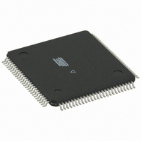
ATMEGA1280V-8AUR Atmel, ATMEGA1280V-8AUR Datasheet - Page 182

ATMEGA1280V-8AUR
Manufacturer Part Number
ATMEGA1280V-8AUR
Description
MCU AVR 128K FLASH 8MHZ 100TQFP
Manufacturer
Atmel
Series
AVR® ATmegar
Specifications of ATMEGA1280V-8AUR
Core Processor
AVR
Core Size
8-Bit
Speed
8MHz
Connectivity
EBI/EMI, I²C, SPI, UART/USART
Peripherals
Brown-out Detect/Reset, POR, PWM, WDT
Number Of I /o
86
Program Memory Size
128KB (64K x 16)
Program Memory Type
FLASH
Eeprom Size
4K x 8
Ram Size
8K x 8
Voltage - Supply (vcc/vdd)
1.8 V ~ 5.5 V
Data Converters
A/D 16x10b
Oscillator Type
Internal
Operating Temperature
-40°C ~ 85°C
Package / Case
100-TQFP, 100-VQFP
For Use With
ATSTK600-TQFP100 - STK600 SOCKET/ADAPTER 100-TQFPATSTK503 - STARTER KIT AVR EXP MODULE 100P
Lead Free Status / RoHS Status
Lead free / RoHS Compliant
Available stocks
Company
Part Number
Manufacturer
Quantity
Price
- Current page: 182 of 444
- Download datasheet (10Mb)
19.6
2549M–AVR–09/10
Compare Match Output Unit
The setup of the OC2x should be performed before setting the Data Direction Register for the
port pin to output. The easiest way of setting the OC2x value is to use the Force Output Com-
pare (FOC2x) strobe bit in Normal mode. The OC2x Register keeps its value even when
changing between Waveform Generation modes.
Be aware that the COM2x1:0 bits are not double buffered together with the compare value.
Changing the COM2x1:0 bits will take effect immediately.
The Compare Output mode (COM2x1:0) bits have two functions. The Waveform Generator uses
the COM2x1:0 bits for defining the Output Compare (OC2x) state at the next compare match.
Also, the COM2x1:0 bits control the OC2x pin output source.
schematic of the logic affected by the COM2x1:0 bit setting. The I/O Registers, I/O bits, and I/O
pins in the figure are shown in bold. Only the parts of the general I/O Port Control Registers
(DDR and PORT) that are affected by the COM2x1:0 bits are shown. When referring to the
OC2x state, the reference is for the internal OC2x Register, not the OC2x pin.
Figure 19-7. Compare Match Output Unit, Schematic
The general I/O port function is overridden by the Output Compare (OC2x) from the Waveform
Generator if either of the COM2x1:0 bits are set. However, the OC2x pin direction (input or out-
put) is still controlled by the Data Direction Register (DDR) for the port pin. The Data Direction
Register bit for the OC2x pin (DDR_OC2x) must be set as output before the OC2x value is visi-
ble on the pin. The port override function is independent of the Waveform Generation mode.
The design of the Output Compare pin logic allows initialization of the OC2x state before the out-
put is enabled. Note that some COM2x1:0 bit settings are reserved for certain modes of
operation.
COMnx1
COMnx0
FOCnx
clk
I/O
See “Register Description” on page 187.
Waveform
Generator
ATmega640/1280/1281/2560/2561
D
D
PORT
D
DDR
OCnx
Q
Q
Q
Figure 19-7
1
0
shows a simplified
OCnx
Pin
182
Related parts for ATMEGA1280V-8AUR
Image
Part Number
Description
Manufacturer
Datasheet
Request
R

Part Number:
Description:
Manufacturer:
Atmel Corporation
Datasheet:

Part Number:
Description:
IC MCU AVR 128K FLASH 100-CBGA
Manufacturer:
Atmel
Datasheet:

Part Number:
Description:
IC MCU AVR 128K FLASH 100-TQFP
Manufacturer:
Atmel
Datasheet:

Part Number:
Description:
MCU AVR 128K FLASH 16MHZ 100TQFP
Manufacturer:
Atmel
Datasheet:

Part Number:
Description:
MCU AVR 128K FLASH 16MHZ 100CBGA
Manufacturer:
Atmel
Datasheet:

Part Number:
Description:
Manufacturer:
ATMEL Corporation
Datasheet:

Part Number:
Description:
Microcontroller with 128K bytes In-system programmable flash, 8 MHz, power supply =2.7 - 5.5V
Manufacturer:
ATMEL Corporation
Datasheet:

Part Number:
Description:
IC AVR MCU 128K 16MHZ 5V 64TQFP
Manufacturer:
Atmel
Datasheet:

Part Number:
Description:
IC AVR MCU 128K 16MHZ 5V 64-QFN
Manufacturer:
Atmel
Datasheet:

Part Number:
Description:
IC AVR MCU 128K 16MHZ COM 64-QFN
Manufacturer:
Atmel
Datasheet:

Part Number:
Description:
IC AVR MCU 128K 16MHZ 64-TQFP
Manufacturer:
Atmel
Datasheet:


