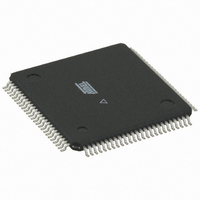
ATMEGA1280V-8AUR Atmel, ATMEGA1280V-8AUR Datasheet - Page 91

ATMEGA1280V-8AUR
Manufacturer Part Number
ATMEGA1280V-8AUR
Description
MCU AVR 128K FLASH 8MHZ 100TQFP
Manufacturer
Atmel
Series
AVR® ATmegar
Specifications of ATMEGA1280V-8AUR
Core Processor
AVR
Core Size
8-Bit
Speed
8MHz
Connectivity
EBI/EMI, I²C, SPI, UART/USART
Peripherals
Brown-out Detect/Reset, POR, PWM, WDT
Number Of I /o
86
Program Memory Size
128KB (64K x 16)
Program Memory Type
FLASH
Eeprom Size
4K x 8
Ram Size
8K x 8
Voltage - Supply (vcc/vdd)
1.8 V ~ 5.5 V
Data Converters
A/D 16x10b
Oscillator Type
Internal
Operating Temperature
-40°C ~ 85°C
Package / Case
100-TQFP, 100-VQFP
For Use With
ATSTK600-TQFP100 - STK600 SOCKET/ADAPTER 100-TQFPATSTK503 - STARTER KIT AVR EXP MODULE 100P
Lead Free Status / RoHS Status
Lead free / RoHS Compliant
Available stocks
Company
Part Number
Manufacturer
Quantity
Price
- Current page: 91 of 444
- Download datasheet (10Mb)
2549M–AVR–09/10
• OC0B – Port G, Bit 5
OC0B, Output Compare match B output: The PG5 pin can serve as an external output for the
TImer/Counter0 Output Compare. The pin has to be configured as an output (DDG5 set) to
serve this function. The OC0B pin is also the output pin for the PWM mode timer function.
• TOSC1 – Port G, Bit 4
TOSC2, Timer Oscillator pin 1: When the AS2 bit in ASSR is set (one) to enable asynchronous
clocking of Timer/Counter2, pin PG4 is disconnected from the port, and becomes the input of the
inverting Oscillator amplifier. In this mode, a Crystal Oscillator is connected to this pin, and the
pin can not be used as an I/O pin.
• TOSC2 – Port G, Bit 3
TOSC2, Timer Oscillator pin 2: When the AS2 bit in ASSR is set (one) to enable asynchronous
clocking of Timer/Counter2, pin PG3 is disconnected from the port, and becomes the inverting
output of the Oscillator amplifier. In this mode, a Crystal Oscillator is connected to this pin, and
the pin can not be used as an I/O pin.
• ALE – Port G, Bit 2
ALE is the external data memory Address Latch Enable signal.
• RD – Port G, Bit 1
RD is the external data memory read control strobe.
• WR – Port G, Bit 0
WR is the external data memory write control strobe.
Table 12-22 on page 91
the overriding signals shown in
Table 12-22. Overriding Signals for Alternate Functions in PG5:PG4
Signal Name
DIEOE
DIEOV
PUOE
DDOE
DDOV
PUOV
PVOE
PVOV
PTOE
AIO
DI
and
—
–
–
–
–
–
–
–
–
–
–
–
Table 12-23 on page 92
Figure 12-5 on page
ATmega640/1280/1281/2560/2561
—
–
–
–
–
–
–
–
–
–
–
–
76.
relates the alternate functions of Port G to
OC0B Enable
PG5/OC0B
OC0B
–
–
–
–
–
–
–
–
–
T/C2 OSC INPUT
PG4/TOSC1
EXCLK
AS2
AS2
AS2
0
0
0
0
–
–
91
Related parts for ATMEGA1280V-8AUR
Image
Part Number
Description
Manufacturer
Datasheet
Request
R

Part Number:
Description:
Manufacturer:
Atmel Corporation
Datasheet:

Part Number:
Description:
IC MCU AVR 128K FLASH 100-CBGA
Manufacturer:
Atmel
Datasheet:

Part Number:
Description:
IC MCU AVR 128K FLASH 100-TQFP
Manufacturer:
Atmel
Datasheet:

Part Number:
Description:
MCU AVR 128K FLASH 16MHZ 100TQFP
Manufacturer:
Atmel
Datasheet:

Part Number:
Description:
MCU AVR 128K FLASH 16MHZ 100CBGA
Manufacturer:
Atmel
Datasheet:

Part Number:
Description:
Manufacturer:
ATMEL Corporation
Datasheet:

Part Number:
Description:
Microcontroller with 128K bytes In-system programmable flash, 8 MHz, power supply =2.7 - 5.5V
Manufacturer:
ATMEL Corporation
Datasheet:

Part Number:
Description:
IC AVR MCU 128K 16MHZ 5V 64TQFP
Manufacturer:
Atmel
Datasheet:

Part Number:
Description:
IC AVR MCU 128K 16MHZ 5V 64-QFN
Manufacturer:
Atmel
Datasheet:

Part Number:
Description:
IC AVR MCU 128K 16MHZ COM 64-QFN
Manufacturer:
Atmel
Datasheet:

Part Number:
Description:
IC AVR MCU 128K 16MHZ 64-TQFP
Manufacturer:
Atmel
Datasheet:


