P89V51RB2BBC,557 NXP Semiconductors, P89V51RB2BBC,557 Datasheet - Page 6
P89V51RB2BBC,557
Manufacturer Part Number
P89V51RB2BBC,557
Description
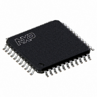
IC 80C51 MCU 1024 RAM 44TQFP
Manufacturer
NXP Semiconductors
Series
89Vr
Datasheet
1.P89V51RC2FBC557.pdf
(80 pages)
Specifications of P89V51RB2BBC,557
Program Memory Type
FLASH
Program Memory Size
16KB (16K x 8)
Package / Case
44-TQFP, 44-VQFP
Core Processor
8051
Core Size
8-Bit
Speed
40MHz
Connectivity
SPI, UART/USART
Peripherals
Brown-out Detect/Reset, POR, PWM, WDT
Number Of I /o
32
Ram Size
1K x 8
Voltage - Supply (vcc/vdd)
4.5 V ~ 5.5 V
Oscillator Type
Internal
Operating Temperature
0°C ~ 70°C
Processor Series
P89V5x
Core
80C51
Data Bus Width
8 bit
Data Ram Size
1 KB
Interface Type
SPI, UART
Maximum Clock Frequency
40 MHz
Number Of Programmable I/os
32
Number Of Timers
3
Maximum Operating Temperature
+ 70 C
Mounting Style
SMD/SMT
3rd Party Development Tools
PK51, CA51, A51, ULINK2
Minimum Operating Temperature
0 C
Lead Free Status / RoHS Status
Lead free / RoHS Compliant
For Use With
622-1017 - BOARD 44-ZIF PLCC SOCKET
Eeprom Size
-
Data Converters
-
Lead Free Status / Rohs Status
Lead free / RoHS Compliant
Other names
935277723557
P89V51RB2BBC
P89V51RB2BBC
P89V51RB2BBC
P89V51RB2BBC
Available stocks
Company
Part Number
Manufacturer
Quantity
Price
Company:

Part Number:
P89V51RB2BBC,557
Manufacturer:
NXP Semiconductors
Quantity:
10 000


NXP Semiconductors
Table 3.
P89V51RB2_RC2_RD2_5
Product data sheet
Symbol
P0.0 to P0.7
P0.0/AD0
P0.1/AD1
P0.2/AD2
P0.3/AD3
P0.4/AD4
P0.5/AD5
P0.6/AD6
P0.7/AD7
P1.0 to P1.7
P1.0/T2
P1.1/T2EX
P89V51RB2/RC2/RD2 pin description
Pin
DIP40
39
38
37
36
35
34
33
32
1
2
5.2 Pin description
TQFP44
37
36
35
34
33
32
31
30
40
41
PLCC44
43
42
41
40
39
38
37
36
2
3
Rev. 05 — 12 November 2009
Type
I/O
I/O
I/O
I/O
I/O
I/O
I/O
I/O
I/O
I/O
I/O
I/O
I/O
I/O
I/O
I/O
I/O
I/O with
internal
pull-up
I/O
I/O
I/O
I
Description
Port 0: Port 0 is an 8-bit open drain bidirectional I/O port.
Port 0 pins that have ‘1’s written to them float, and in this
state can be used as high-impedance inputs. Port 0 is also
the multiplexed low-order address and data bus during
accesses to external code and data memory. In this
application, it uses strong internal pull-ups when
transitioning to ‘1’s. Port 0 also receives the code bytes
during the external host mode programming, and outputs
the code bytes during the external host mode verification.
External pull-ups are required during program verification
or as a general purpose I/O port.
P0.0 — Port 0 bit 0.
AD0 — Address/data bit 0.
P0.1 — Port 0 bit 1.
AD1 — Address/data bit 1.
P0.2 — Port 0 bit 2.
AD2 — Address/data bit 2.
P0.3 — Port 0 bit 3.
AD3 — Address/data bit 3.
P0.4 — Port 0 bit 4.
AD4 — Address/data bit 4.
P0.5 — Port 0 bit 5.
AD5 — Address/data bit 5.
P0.6 — Port 0 bit 6.
AD6 — Address/data bit 6.
P0.7 — Port 0 bit 7.
AD7 — Address/data bit 7.
Port 1: Port 1 is an 8-bit bidirectional I/O port with internal
pull-ups. The Port 1 pins are pulled high by the internal
pull-ups when ‘1’s are written to them and can be used as
inputs in this state. As inputs, Port 1 pins that are
externally pulled LOW will source current (I
the internal pull-ups. P1.5, P1.6, P1.7 have high current
drive of 16 mA. Port 1 also receives the low-order address
bytes during the external host mode programming and
verification.
P1.0 — Port 1 bit 0.
T2 — External count input to Timer/counter 2 or Clock-out
from Timer/counter 2.
P1.1 — Port 1 bit 1.
T2EX: Timer/counter 2 capture/reload trigger and direction
control.
P89V51RB2/RC2/RD2
8-bit microcontrollers with 80C51 core
© NXP B.V. 2009. All rights reserved.
IL
) because of
6 of 80
Related parts for P89V51RB2BBC,557
Image
Part Number
Description
Manufacturer
Datasheet
Request
R

Part Number:
Description:
8-bit 80c51 5 V Low Power 16/32/64 Kb Flash Microcontroller With 1 Kb Ram
Manufacturer:
NXP Semiconductors
Datasheet:
Part Number:
Description:
NXP Semiconductors designed the LPC2420/2460 microcontroller around a 16-bit/32-bitARM7TDMI-S CPU core with real-time debug interfaces that include both JTAG andembedded trace
Manufacturer:
NXP Semiconductors
Datasheet:

Part Number:
Description:
NXP Semiconductors designed the LPC2458 microcontroller around a 16-bit/32-bitARM7TDMI-S CPU core with real-time debug interfaces that include both JTAG andembedded trace
Manufacturer:
NXP Semiconductors
Datasheet:
Part Number:
Description:
NXP Semiconductors designed the LPC2468 microcontroller around a 16-bit/32-bitARM7TDMI-S CPU core with real-time debug interfaces that include both JTAG andembedded trace
Manufacturer:
NXP Semiconductors
Datasheet:
Part Number:
Description:
NXP Semiconductors designed the LPC2470 microcontroller, powered by theARM7TDMI-S core, to be a highly integrated microcontroller for a wide range ofapplications that require advanced communications and high quality graphic displays
Manufacturer:
NXP Semiconductors
Datasheet:
Part Number:
Description:
NXP Semiconductors designed the LPC2478 microcontroller, powered by theARM7TDMI-S core, to be a highly integrated microcontroller for a wide range ofapplications that require advanced communications and high quality graphic displays
Manufacturer:
NXP Semiconductors
Datasheet:
Part Number:
Description:
The Philips Semiconductors XA (eXtended Architecture) family of 16-bit single-chip microcontrollers is powerful enough to easily handle the requirements of high performance embedded applications, yet inexpensive enough to compete in the market for hi
Manufacturer:
NXP Semiconductors
Datasheet:
Part Number:
Description:
The XA-S3 device is a member of Philips Semiconductors? XA(eXtended Architecture) family of high performance 16-bitsingle-chip microcontrollers
Manufacturer:
NXP Semiconductors
Datasheet:

Part Number:
Description:
The NXP BlueStreak LH75401/LH75411 family consists of two low-cost 16/32-bit System-on-Chip (SoC) devices
Manufacturer:
NXP Semiconductors
Datasheet:
Part Number:
Description:
The NXP LPC3130/3131 combine an 180 MHz ARM926EJ-S CPU core, high-speed USB2
Manufacturer:
NXP Semiconductors
Datasheet:
Part Number:
Description:
The NXP LPC3141 combine a 270 MHz ARM926EJ-S CPU core, High-speed USB 2
Manufacturer:
NXP Semiconductors
Part Number:
Description:
The NXP LPC3143 combine a 270 MHz ARM926EJ-S CPU core, High-speed USB 2
Manufacturer:
NXP Semiconductors

Part Number:
Description:
The NXP LPC3152 combines an 180 MHz ARM926EJ-S CPU core, High-speed USB 2
Manufacturer:
NXP Semiconductors
Part Number:
Description:
The NXP LPC3154 combines an 180 MHz ARM926EJ-S CPU core, High-speed USB 2
Manufacturer:
NXP Semiconductors