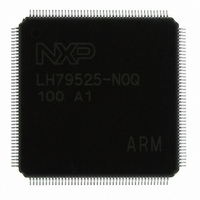
LH79525N0Q100A1;55 NXP Semiconductors, LH79525N0Q100A1;55 Datasheet - Page 35

LH79525N0Q100A1;55
Manufacturer Part Number
LH79525N0Q100A1;55
Description
IC ARM7 BLUESTREAK MCU 176LQFP
Manufacturer
NXP Semiconductors
Series
BlueStreak ; LH7r
Datasheet
1.LH79524N0F100A155.pdf
(64 pages)
Specifications of LH79525N0Q100A1;55
Package / Case
176-LQFP
Core Processor
ARM7
Core Size
32-Bit
Speed
76.2MHz
Connectivity
EBI/EMI, Ethernet, I²C, IrDA, Microwire, SPI, SSI, SSP, UART/USART, USB
Peripherals
Brown-out Detect/Reset, DMA, I²S, LCD, POR, PWM, WDT
Number Of I /o
86
Program Memory Type
ROMless
Ram Size
16K x 8
Voltage - Supply (vcc/vdd)
1.7 V ~ 3.6 V
Data Converters
A/D 10x10b
Oscillator Type
External
Operating Temperature
-40°C ~ 85°C
Processor Series
LH795
Core
RISC
Data Bus Width
16 bit
Data Ram Size
16 KB
Interface Type
I2C, UART
Maximum Clock Frequency
50.803 MHz
Number Of Timers
4
Operating Supply Voltage
3.3 V
Maximum Operating Temperature
+ 85 C
Mounting Style
SMD/SMT
3rd Party Development Tools
MDK-ARM, RL-ARM, ULINK2
Minimum Operating Temperature
- 40 C
Lead Free Status / RoHS Status
Lead free / RoHS Compliant
Eeprom Size
-
Program Memory Size
-
Lead Free Status / Rohs Status
Lead free / RoHS Compliant
Other names
568-4333
935285052557
LH79525N0Q100A1
935285052557
LH79525N0Q100A1
System-on-Chip
NOTES:
1. The timing relationship is specified as a cycle-based timing. Variations caused by clock jitter, power rail noise, and I/O conditioning will cause
2. The Read Wait States register (SWAITRDx) must be set to a minimum value of 3.
3. For each rising clock edge (HCLK) that the assertion of nWAIT lags the assertion of nCSx, another read wait state (SWAITRDx) must be
4. nWAIT delay cycles are not added for all nWAIT assertions sampled prior to WST-3. These nWAIT assertions are ignored.
5. nWAIT delay cycles are added for all nWAIT assertions sampled from WST-3 until the de-assertion of nWAIT. nWAIT delay cycles are added
6. Once nWAIT is sampled high, the current memory transaction is queued to complete.
7. Since static and dynamic memory cannot be accessed at the same time, any prolonged access (either due to nWAIT or the Extended Wait
8. Timing assumes Output Enable Delay register (SWAITOENx) is programmed to 0.
Preliminary data sheet
tDA_nCS(x)_nWAIT
tDD_nWAIT_nCS(x)
tDD_nWAIT_nOE
tA_nWAIT
NOTES:
SQ: nWAIT Sampled and Queued
SI: nWAIT Sampled and Ignored
these timings to vary nominally. It is recommended that designers add a small margin to avoid possible corner-case conditions.
added to the minimum requirement.
once the wait state countdown has reached WST-1.
Register) that causes an SDRAM refresh failure may cause SDRAM data to be lost.
nCS(x)
nWAIT
HCLK
Transaction
Sequence
nOE
PARAMETER
tDA_nCS(x)_nWAIT
DELAY
WST-3
Delay from nCS(x) assertion to nWAIT assertion
Delay from nWAIT deassertion to nCS(x) deassertion
Delay from nWAIT deassertion to nOE deassertion
Assertion time of nWAIT
SQ-4
Table 16. nWAIT Read Sequence Parameter Definitions
DELAY
WST-2
Figure 11. nWAIT Read Sequence (SWAITRDx = 3)
SQ-3
DELAY
WST-1
tA_nWAIT
SQ-2
NXP Semiconductors
DELAY
nWAIT
Rev. 01 — 16 July 2007
SQ-4
DESCRIPTION
SQ-1
DELAY
nWAIT
SQ-3
SQ-0
DELAY
nWAIT
SQ-2
DELAY
nWAIT
tDD_nWAIT_nCS(x)
SQ-1
tDD_nWAIT_nOE
DELAY
nWAIT
SQ-0
MIN.
0
2
DELAY
WST-0
16,365
MAX.
4
4
LH79524/LH79525
HCLK periods
HCLK periods
HCLK periods
HCLK periods
UNIT
LH79525-133
1
35


