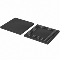
LPC3180FEL320/01,5 NXP Semiconductors, LPC3180FEL320/01,5 Datasheet - Page 14

LPC3180FEL320/01,5
Manufacturer Part Number
LPC3180FEL320/01,5
Description
IC ARM9 MCU 208MHZ 320-LFBGA
Manufacturer
NXP Semiconductors
Series
LPC3000r
Specifications of LPC3180FEL320/01,5
Package / Case
320-LFBGA
Core Processor
ARM9
Core Size
16/32-Bit
Speed
208MHz
Connectivity
EBI/EMI, I²C, MMC, SPI, UART/USART, USB OTG
Peripherals
DMA, PWM, WDT
Number Of I /o
55
Program Memory Type
ROMless
Ram Size
64K x 8
Voltage - Supply (vcc/vdd)
1.1 V ~ 3.3 V
Data Converters
A/D 3x10b
Oscillator Type
External
Operating Temperature
-40°C ~ 85°C
Processor Series
LPC31
Core
ARM926EJ-S
Data Bus Width
32 bit
Maximum Clock Frequency
208 MHz
Operating Supply Voltage
1.8 V / 3V
Maximum Operating Temperature
+ 85 C
Mounting Style
SMD/SMT
3rd Party Development Tools
MDK-ARM, RL-ARM, ULINK2
Development Tools By Supplier
OM10096
Minimum Operating Temperature
- 40 C
Package
320LFBGA
Device Core
ARM926EJ-S
Family Name
LPC3100
Maximum Speed
208 MHz
Number Of Programmable I/os
55
Interface Type
I2C/SPI/UART/USB
On-chip Adc
3-chx10-bit
Number Of Timers
2
Lead Free Status / RoHS Status
Lead free / RoHS Compliant
For Use With
622-1018 - EVAL KIT FOR LP3180568-4063 - KIT DEV LPC3180568-4062 - DEBUGGER J-LINK JTAG568-4061 - DEBUGGER U-LINK2 JTAG FOR NXP
Eeprom Size
-
Program Memory Size
-
Lead Free Status / Rohs Status
Lead free / RoHS Compliant
Other names
568-4529
935286983551
935286983551
Available stocks
Company
Part Number
Manufacturer
Quantity
Price
Company:
Part Number:
LPC3180FEL320/01,5
Manufacturer:
NXP Semiconductors
Quantity:
10 000
NXP Semiconductors
LPC3180_01_1
Preliminary data sheet
6.3 AHB matrix
6.4 On-chip SRAM
6.5 Memory map
The microcontroller has a multi-layer AHB matrix for inter-block communication. AHB is
the ARM high-speed bus, which is part of the ARM bus architecture. AHB is a
high-bandwidth low-latency bus that supports multi-master arbitration and a bus
grant/request mechanism. For systems where there is only one bus master (the CPU), or
where there are two masters (CPU and DMA) and the CPU does not generally need to
contend with the DMA for program memory access (because the CPU has access to
memory on its local bus or has caches or another AHB bus etc.), this arrangement works
well. However, if there are multiple bus masters and the CPU needs access to external
memory, a single AHB bus can cause a bottleneck. ARM’s solution to this was to invent a
multi-layer AHB which replaces the request/grant and arbitration mechanism with a
multiplexer fabric that pushes arbitration to the level of the devices. Thus, if a CPU and a
DMA controller want access to the same memory, the multi-layer fabric will arbitrate
between the two on granting access to that memory. This allows simultaneous access by
bus masters to different resources at the cost of increased arbitration complexity. As with
all trade-offs, the pros and cons must be analyzed, for a microcontroller operating at
200 MHz, removing guaranteed central arbitration in case more than one bus master is
active in favor of occasional local arbitration gives better performance.
The blocks outside the CPU can be roughly split into memory controllers, serial
communication, I/O, timers/counters and RTC, system control, and debug and trace
blocks. These are described as follows.
On-chip SRAM may be used for code and/or data storage. The SRAM may be accessed
as 8/16/32 bit. The LPC3180/01 provides 64 kB of SRAM.
The LPC3180/01 memory map incorporates several distinct regions, as shown in
Figure
allow them to reside in on-chip SRAM.
3. When an application is running, the CPU interrupt vectors are re-mapped to
Rev. 00.08 — 20 November 2008
16/32-bit ARM microcontroller with external memory interface
LPC3180/01
© NXP B.V. 2008. All rights reserved.
14 of 56


