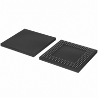
LPC3180FEL320/01,5 NXP Semiconductors, LPC3180FEL320/01,5 Datasheet - Page 18

LPC3180FEL320/01,5
Manufacturer Part Number
LPC3180FEL320/01,5
Description
IC ARM9 MCU 208MHZ 320-LFBGA
Manufacturer
NXP Semiconductors
Series
LPC3000r
Specifications of LPC3180FEL320/01,5
Package / Case
320-LFBGA
Core Processor
ARM9
Core Size
16/32-Bit
Speed
208MHz
Connectivity
EBI/EMI, I²C, MMC, SPI, UART/USART, USB OTG
Peripherals
DMA, PWM, WDT
Number Of I /o
55
Program Memory Type
ROMless
Ram Size
64K x 8
Voltage - Supply (vcc/vdd)
1.1 V ~ 3.3 V
Data Converters
A/D 3x10b
Oscillator Type
External
Operating Temperature
-40°C ~ 85°C
Processor Series
LPC31
Core
ARM926EJ-S
Data Bus Width
32 bit
Maximum Clock Frequency
208 MHz
Operating Supply Voltage
1.8 V / 3V
Maximum Operating Temperature
+ 85 C
Mounting Style
SMD/SMT
3rd Party Development Tools
MDK-ARM, RL-ARM, ULINK2
Development Tools By Supplier
OM10096
Minimum Operating Temperature
- 40 C
Package
320LFBGA
Device Core
ARM926EJ-S
Family Name
LPC3100
Maximum Speed
208 MHz
Number Of Programmable I/os
55
Interface Type
I2C/SPI/UART/USB
On-chip Adc
3-chx10-bit
Number Of Timers
2
Lead Free Status / RoHS Status
Lead free / RoHS Compliant
For Use With
622-1018 - EVAL KIT FOR LP3180568-4063 - KIT DEV LPC3180568-4062 - DEBUGGER J-LINK JTAG568-4061 - DEBUGGER U-LINK2 JTAG FOR NXP
Eeprom Size
-
Program Memory Size
-
Lead Free Status / Rohs Status
Lead free / RoHS Compliant
Other names
568-4529
935286983551
935286983551
Available stocks
Company
Part Number
Manufacturer
Quantity
Price
Company:
Part Number:
LPC3180FEL320/01,5
Manufacturer:
NXP Semiconductors
Quantity:
10 000
NXP Semiconductors
LPC3180_01_1
Preliminary data sheet
6.12.1.1 Features
6.12.2.1 Features
6.12.1 USB device controller
6.12.2 USB host controller
6.12 USB interface
The LPC3180/01 supports USB in either device, host, or OTG configuration.
The USB device controller enables 12 Mbit/s data exchange with a USB host controller. It
consists of register interface, serial interface engine, endpoint buffer memory and DMA
controller. The serial interface engine decodes the USB data stream and writes data to the
appropriate end point buffer memory. The status of a completed USB transfer or error
condition is indicated via status registers. An interrupt is also generated if enabled. The
DMA controller when enabled transfers data between the endpoint buffer and the USB
RAM.
The host controller enables data exchange with various USB devices attached to the bus.
It consists of register interface, serial interface engine and DMA controller. The register
interface complies to the OHCI specification.
•
•
•
•
•
•
•
•
•
•
•
•
•
•
•
•
•
Uses 32 kHz RTC clock
Fully compliant with USB 2.0 full-speed specification.
Supports 32 physical (16 logical) endpoints.
Supports control, bulk, interrupt and isochronous endpoints.
Scalable realization of endpoints at run time.
Endpoint maximum packet size selection (up to USB maximum specification) by
software at run time.
RAM message buffer size based on endpoint realization and maximum packet size.
Supports bus-powered capability with low suspend current.
Supports DMA transfer on all non-control endpoints.
One duplex DMA channel serves all endpoints.
Allows dynamic switching between CPU controlled and DMA modes.
Double buffer implementation for bulk and isochronous endpoints.
OHCI compliant.
OHCI specifies the operation and interface of the USB host controller and SW driver.
The host controller has four USB states visible to the SW driver:
– USBOperational: Process lists and generate SOF tokens.
– USBReset: Forces reset signaling on the bus, SOF disabled.
– USBSuspend: Monitor USB for wake-up activity.
– USBResume: Forces resume signaling on the bus.
HCCA register points to interrupt and isochronous descriptors list.
ControlHeadED and BulkHeadED registers point to control and bulk descriptors list.
Rev. 00.08 — 20 November 2008
16/32-bit ARM microcontroller with external memory interface
LPC3180/01
© NXP B.V. 2008. All rights reserved.
18 of 56


