ST7FLI49MK1T6 STMicroelectronics, ST7FLI49MK1T6 Datasheet - Page 37
ST7FLI49MK1T6
Manufacturer Part Number
ST7FLI49MK1T6
Description
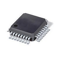
MCU 8BIT SGL VOLT FLASH 32-LQFP
Manufacturer
STMicroelectronics
Series
ST7r
Datasheet
1.ST7FLI49MK1T6TR.pdf
(187 pages)
Specifications of ST7FLI49MK1T6
Core Processor
ST7
Core Size
8-Bit
Speed
8MHz
Connectivity
I²C
Peripherals
LVD, POR, PWM, WDT
Number Of I /o
24
Program Memory Size
4KB (4K x 8)
Program Memory Type
FLASH
Eeprom Size
128 x 8
Ram Size
384 x 8
Voltage - Supply (vcc/vdd)
2.4 V ~ 5.5 V
Data Converters
A/D 10x10b
Oscillator Type
Internal
Operating Temperature
-40°C ~ 85°C
Package / Case
32-LQFP
Processor Series
ST7FLI4x
Core
ST7
Data Bus Width
8 bit
Data Ram Size
384 B
Interface Type
I2C
Maximum Clock Frequency
8 MHz
Number Of Programmable I/os
24
Number Of Timers
5
Maximum Operating Temperature
+ 125 C
Mounting Style
SMD/SMT
Minimum Operating Temperature
- 40 C
On-chip Adc
10 bit, 10 Channel
Lead Free Status / RoHS Status
Lead free / RoHS Compliant
Available stocks
Company
Part Number
Manufacturer
Quantity
Price
Company:

Part Number:
ST7FLI49MK1T6
Manufacturer:
st
Quantity:
456
Company:
Part Number:
ST7FLI49MK1T6
Manufacturer:
STMicroelectronics
Quantity:
10 000
Part Number:
ST7FLI49MK1T6
Manufacturer:
ST
Quantity:
20 000
Company:
Part Number:
ST7FLI49MK1T6TR
Manufacturer:
STMicroelectronics
Quantity:
10 000


ST7LITE49M
7.3
7.3.1
Note:
Table 6.
Reset sequence manager (RSM)
Introduction
The reset sequence manager includes three RESET sources as shown in
●
●
●
A reset can also be triggered following the detection of an illegal opcode or prebyte code.
Refer to
These sources act on the RESET pin and it is always kept low during the delay phase.
The RESET service routine vector is fixed at addresses FFFEh-FFFFh in the ST7 memory
mapping.
The basic RESET sequence consists of 3 phases as shown in
●
●
External RESET source pulse
Internal LVD RESET (low voltage detection)
Internal WATCHDOG RESET
Active phase depending on the RESET source
256 CPU clock cycle delay (see
Section 12.2.1 on page 136
ST7 clock sources
Doc ID 13562 Rev 3
for further details.
Table
Hardware configuration
C
L1
EXTERNAL
SOURCE
OSC1
OSC1
OSC1
7)
CAPACITORS
LOAD
ST7
ST7
ST7
Supply, reset and clock management
OSC2
OSC2
OSC2
C
L2
Figure
14:
Figure
15:
37/188
Related parts for ST7FLI49MK1T6
Image
Part Number
Description
Manufacturer
Datasheet
Request
R

Part Number:
Description:
BOARD DAUGHTER 32LQFP ST7FLITE4
Manufacturer:
STMicroelectronics
Datasheet:
Part Number:
Description:
STMicroelectronics [RIPPLE-CARRY BINARY COUNTER/DIVIDERS]
Manufacturer:
STMicroelectronics
Datasheet:
Part Number:
Description:
STMicroelectronics [LIQUID-CRYSTAL DISPLAY DRIVERS]
Manufacturer:
STMicroelectronics
Datasheet:

Part Number:
Description:
BOARD EVAL FOR MEMS SENSORS
Manufacturer:
STMicroelectronics
Datasheet:
Part Number:
Description:
NPN TRANSISTOR POWER MODULE
Manufacturer:
STMicroelectronics
Datasheet:
Part Number:
Description:
TURBOSWITCH ULTRA-FAST HIGH VOLTAGE DIODE
Manufacturer:
STMicroelectronics
Datasheet:
Part Number:
Description:
Manufacturer:
STMicroelectronics
Datasheet:
Part Number:
Description:
DIODE / SCR MODULE
Manufacturer:
STMicroelectronics
Datasheet:
Part Number:
Description:
DIODE / SCR MODULE
Manufacturer:
STMicroelectronics
Datasheet:
Part Number:
Description:
Search -----> STE16N100
Manufacturer:
STMicroelectronics
Datasheet:
Part Number:
Description:
Search ---> STE53NA50
Manufacturer:
STMicroelectronics
Datasheet:
Part Number:
Description:
NPN Transistor Power Module
Manufacturer:
STMicroelectronics
Datasheet: