ST7FLI49MK1T6 STMicroelectronics, ST7FLI49MK1T6 Datasheet - Page 44
ST7FLI49MK1T6
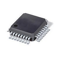
Manufacturer Part Number
ST7FLI49MK1T6
Description
MCU 8BIT SGL VOLT FLASH 32-LQFP
Manufacturer
STMicroelectronics
Series
ST7r
Datasheet
1.ST7FLI49MK1T6TR.pdf
(187 pages)
Specifications of ST7FLI49MK1T6
Core Processor
ST7
Core Size
8-Bit
Speed
8MHz
Connectivity
I²C
Peripherals
LVD, POR, PWM, WDT
Number Of I /o
24
Program Memory Size
4KB (4K x 8)
Program Memory Type
FLASH
Eeprom Size
128 x 8
Ram Size
384 x 8
Voltage - Supply (vcc/vdd)
2.4 V ~ 5.5 V
Data Converters
A/D 10x10b
Oscillator Type
Internal
Operating Temperature
-40°C ~ 85°C
Package / Case
32-LQFP
Processor Series
ST7FLI4x
Core
ST7
Data Bus Width
8 bit
Data Ram Size
384 B
Interface Type
I2C
Maximum Clock Frequency
8 MHz
Number Of Programmable I/os
24
Number Of Timers
5
Maximum Operating Temperature
+ 125 C
Mounting Style
SMD/SMT
Minimum Operating Temperature
- 40 C
On-chip Adc
10 bit, 10 Channel
Lead Free Status / RoHS Status
Lead free / RoHS Compliant
Available stocks
Company
Part Number
Manufacturer
Quantity
Price
Company:

Part Number:
ST7FLI49MK1T6
Manufacturer:
st
Quantity:
456
Company:
Part Number:
ST7FLI49MK1T6
Manufacturer:
STMicroelectronics
Quantity:
10 000
Part Number:
ST7FLI49MK1T6
Manufacturer:
ST
Quantity:
20 000
Company:
Part Number:
ST7FLI49MK1T6TR
Manufacturer:
STMicroelectronics
Quantity:
10 000


Supply, reset and clock management
7.5
7.5.1
7.5.2
Note:
44/188
Register description
Main clock control/status register (MCCSR)
Reset value: 0000 0000 (00h)
Bits 7:2 = Reserved, must be kept cleared.
Bit 1 = MCO Main clock out enable bit
Bit 0 = SMS Slow mode selection bit
RC control register (RCCR)
Reset value: 1111 1111 (FFh)
Bits 7:0 = CR[9:2] RC oscillator frequency adjustment bits
To tune the oscillator, write a series of different values in the register until the correct
frequency is reached. The fastest method is to use a dichotomy starting with 80h.
CR9
This bit is read/write by software and cleared by hardware after a reset. This bit allows
to enable the MCO output clock.
0: MCO clock disabled, I/O port free for general purpose I/O.
1: MCO clock enabled.
This bit is read/write by software and cleared by hardware after a reset. This bit selects
the input clock f
0: Normal mode (f
1: Slow mode (f
These bits must be written immediately after reset to adjust the RC oscillator frequency
and to obtain an accuracy of 1%. The application can store the correct value for each
voltage range in Flash memory and write it to this register at start-up.
00h = maximum available frequency
FFh = lowest available frequency
These bits are used with the CR[1:0] bits in the SICSR register. Refer to
7
0
7
CR8
0
OSC
CPU =
CPU =
or f
f
CR7
OSC
0
OSC
f
OSC
Doc ID 13562 Rev 3
/32)
/32.
CR6
0
Read/write
Read/write
CR5
0
CR4
0
MCO
CR3
Chapter
ST7LITE49M
CR2
SMS
0
0
7.5.3.
Related parts for ST7FLI49MK1T6
Image
Part Number
Description
Manufacturer
Datasheet
Request
R

Part Number:
Description:
BOARD DAUGHTER 32LQFP ST7FLITE4
Manufacturer:
STMicroelectronics
Datasheet:
Part Number:
Description:
STMicroelectronics [RIPPLE-CARRY BINARY COUNTER/DIVIDERS]
Manufacturer:
STMicroelectronics
Datasheet:
Part Number:
Description:
STMicroelectronics [LIQUID-CRYSTAL DISPLAY DRIVERS]
Manufacturer:
STMicroelectronics
Datasheet:

Part Number:
Description:
BOARD EVAL FOR MEMS SENSORS
Manufacturer:
STMicroelectronics
Datasheet:
Part Number:
Description:
NPN TRANSISTOR POWER MODULE
Manufacturer:
STMicroelectronics
Datasheet:
Part Number:
Description:
TURBOSWITCH ULTRA-FAST HIGH VOLTAGE DIODE
Manufacturer:
STMicroelectronics
Datasheet:
Part Number:
Description:
Manufacturer:
STMicroelectronics
Datasheet:
Part Number:
Description:
DIODE / SCR MODULE
Manufacturer:
STMicroelectronics
Datasheet:
Part Number:
Description:
DIODE / SCR MODULE
Manufacturer:
STMicroelectronics
Datasheet:
Part Number:
Description:
Search -----> STE16N100
Manufacturer:
STMicroelectronics
Datasheet:
Part Number:
Description:
Search ---> STE53NA50
Manufacturer:
STMicroelectronics
Datasheet:
Part Number:
Description:
NPN Transistor Power Module
Manufacturer:
STMicroelectronics
Datasheet: