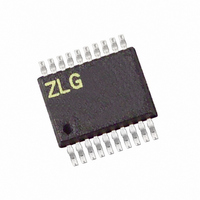
Z86E0208HSG1925 Zilog, Z86E0208HSG1925 Datasheet - Page 14

Z86E0208HSG1925
Manufacturer Part Number
Z86E0208HSG1925
Description
IC Z8 .5K OTP 8MHZ 20-SSOP
Manufacturer
Zilog
Series
Z8®r
Datasheet
1.Z86E0208PSG1925.pdf
(60 pages)
Specifications of Z86E0208HSG1925
Core Processor
Z8
Core Size
8-Bit
Speed
8MHz
Peripherals
POR, WDT
Number Of I /o
14
Program Memory Size
512B (512 x 8)
Program Memory Type
OTP
Ram Size
61 x 8
Voltage - Supply (vcc/vdd)
3.5 V ~ 5.5 V
Oscillator Type
Internal
Operating Temperature
0°C ~ 70°C
Package / Case
20-SSOP
Processor Series
Z86E02x
Core
Z8
Data Bus Width
8 bit
Data Ram Size
61 B
Maximum Clock Frequency
8 MHz
Number Of Programmable I/os
14
Number Of Timers
1
Operating Supply Voltage
4.5 V to 5.5 V
Maximum Operating Temperature
+ 70 C
Mounting Style
SMD/SMT
Minimum Operating Temperature
0 C
Lead Free Status / RoHS Status
Lead free / RoHS Compliant
Eeprom Size
-
Data Converters
-
Connectivity
-
Lead Free Status / Rohs Status
Details
Other names
269-3946
Z86E0208HSG1925
Z86E0208HSG1925
Available stocks
Company
Part Number
Manufacturer
Quantity
Price
Company:
Part Number:
Z86E0208HSG1925
Manufacturer:
Zilog
Quantity:
864
Electrical Characteristics
PS014802-0903
Parameter
Ambient Temperature under Bias
Storage Temperature
Voltage on any Pin with Respect to V
Voltage on V
Voltage on XTAL1, P31, P32, P33 with respect to V
Total Power Dissipation
Maximum Allowable Current out of V
Maximum Allowable Current into V
Maximum Allowable Current into an Input Pin
Maximum Allowable Current into an Open-Drain Pin
Maximum Allowable Output Current Linked by any I/O Pin
Maximum Allowable Output Current Sourced by any I/O Pin
1. Applies to all pins except where otherwise noted. Maximum current into or out of pin must be ±600 µA.
2. Device pin is not at an output Low state.
3. There is no input protection diode from pin to V
4. This excludes XTAL1 and XTAL2.
Absolute Maximum Ratings
Standard Test Conditions
Stresses greater than those listed on Table 6 may cause permanent damage to the device.
This rating is a stress rating only; functional operation of the device at any condition above
those indicated in the operational sections of these specifications is not implied. Exposure
to absolute maximum rating conditions for an extended period may affect device
reliability. Total power dissipation should not exceed 462 mΩ for the package. See
Table 6. Power dissipation is calculated as follows:
The characteristics listed below apply for standard test conditions as noted. All
voltages are referenced to Ground. Positive current flows into the referenced pin
See Figure 7.
DD
Total Power Dissipation =
Pin with Respect to V
Table 6. Absolute Maximum Ratings
DD
SS
SS
SS
V
+sum of [(V
+ sum of (V
DD
CC
General-Purpose OTP MCU with 14 I/O Lines
.
SS
X [I
CC
–(sum of I
CC
OL
Min
-40
-65
-0.7
-0.3
-0.6
-600
-600
–V
X I
OH
OL
) X I
)
OH
)]
OH
Max
+105
+150
+12
+7
V
462
300
270
+600
+600
20
20 mA
DD
]
+1 V
Z86E02 SL 1925
Units
C
C
V
V
mΩ
mA
mA
µA
µA
mA
Note
1
3
4
2
8


