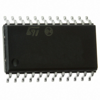
ST72F63BE1M1 STMicroelectronics, ST72F63BE1M1 Datasheet - Page 110

ST72F63BE1M1
Manufacturer Part Number
ST72F63BE1M1
Description
IC MCU 8BIT 4K FLASH 24-SOIC
Manufacturer
STMicroelectronics
Series
ST7r
Datasheet
1.ST72F63BD6U1TR.pdf
(186 pages)
Specifications of ST72F63BE1M1
Core Processor
ST7
Core Size
8-Bit
Speed
8MHz
Connectivity
I²C, SCI, USB
Peripherals
DMA, LVD, POR, PWM, WDT
Number Of I /o
14
Program Memory Size
4KB (4K x 8)
Program Memory Type
FLASH
Ram Size
384 x 8
Voltage - Supply (vcc/vdd)
4 V ~ 5.5 V
Oscillator Type
External
Operating Temperature
0°C ~ 70°C
Package / Case
24-SOIC (7.5mm Width)
Data Converters
A/D 12x8b
Processor Series
ST72F6x
Core
ST7
Data Bus Width
8 bit
Data Ram Size
384 B
Interface Type
I2C, SCI
Maximum Clock Frequency
8 MHz
Number Of Programmable I/os
14
Number Of Timers
1
Maximum Operating Temperature
+ 70 C
Mounting Style
SMD/SMT
Development Tools By Supplier
ST7MDTU3-EPB/US, ST7MDTULS-EVAL, ST72F63B-SK/RAIS, ST7MDTU3-EMU3, STX-RLINK
Minimum Operating Temperature
0 C
For Use With
497-5521 - EVAL BOARD LOW SPEED USB
Lead Free Status / RoHS Status
Lead free / RoHS Compliant
Eeprom Size
-
Lead Free Status / Rohs Status
Details
Available stocks
Company
Part Number
Manufacturer
Quantity
Price
- Current page: 110 of 186
- Download datasheet (3Mb)
On-chip peripherals
110/186
Mode selection
The interface can operate in the four following modes:
●
●
By default, it operates in slave mode.
The interface automatically switches from slave to master after it generates a START
condition and from master to slave in case of arbitration loss or a STOP generation, allowing
then Multi-Master capability.
Communication flow
In Master mode, it initiates a data transfer and generates the clock signal. A serial data
transfer always begins with a start condition and ends with a stop condition. Both start and
stop conditions are generated in master mode by software.
In Slave mode, the interface is capable of recognizing its own address (7-bit), and the
General Call address. The General Call address detection may be enabled or disabled by
software.
Data and addresses are transferred as 8-bit bytes, MSB first. The first byte following the
start condition is the address byte; it is always transmitted in Master mode.
A 9th clock pulse follows the 8 clock cycles of a byte transfer, during which the receiver must
send an acknowledge bit to the transmitter. Refer to
Figure 46. I²C bus protocol
Acknowledge may be enabled and disabled by software.
The I²C interface address and/or general call address can be selected by software.
The speed of the I²C interface may be selected between Standard (up to 100 kHz) and Fast
I²C (up to 400 kHz).
SDA/SCL line control
Transmitter mode: the interface holds the clock line low before transmission to wait for the
microcontroller to write the byte in the Data register.
Receiver mode: the interface holds the clock line low after reception to wait for the
microcontroller to read the byte in the Data register.
The SCL frequency (F
the I²C bus mode.
When the I²C cell is enabled, the SDA and SCL ports must be configured as floating inputs.
In this case, the value of the external pull-up resistor used depends on the application.
Slave transmitter/receiver
Master transmitter/receiver
SCL
SDA
CONDITION
START
SCL
MSB
) is controlled by a programmable clock divider which depends on
1
Doc ID 7516 Rev 8
2
8
Figure
ACK
9
46.
CONDITION
STOP
VR02119B
ST7263Bxx
Related parts for ST72F63BE1M1
Image
Part Number
Description
Manufacturer
Datasheet
Request
R

Part Number:
Description:
KIT STARTER LOW COST ST7
Manufacturer:
STMicroelectronics
Datasheet:

Part Number:
Description:
LOW SPEED USB 8-BIT MCU FAMILY WITH FLASH/ROM, UP TO 512 BYTES RAM, 8-BIT ADC, WDG, TIMER, SCI & I�C
Manufacturer:
STMICROELECTRONICS [STMicroelectronics]
Datasheet:

Part Number:
Description:
STMicroelectronics [RIPPLE-CARRY BINARY COUNTER/DIVIDERS]
Manufacturer:
STMicroelectronics
Datasheet:

Part Number:
Description:
STMicroelectronics [LIQUID-CRYSTAL DISPLAY DRIVERS]
Manufacturer:
STMicroelectronics
Datasheet:

Part Number:
Description:
BOARD EVAL FOR MEMS SENSORS
Manufacturer:
STMicroelectronics
Datasheet:

Part Number:
Description:
NPN TRANSISTOR POWER MODULE
Manufacturer:
STMicroelectronics
Datasheet:

Part Number:
Description:
TURBOSWITCH ULTRA-FAST HIGH VOLTAGE DIODE
Manufacturer:
STMicroelectronics
Datasheet:

Part Number:
Description:
Manufacturer:
STMicroelectronics
Datasheet:

Part Number:
Description:
DIODE / SCR MODULE
Manufacturer:
STMicroelectronics
Datasheet:

Part Number:
Description:
DIODE / SCR MODULE
Manufacturer:
STMicroelectronics
Datasheet:

Part Number:
Description:
Search -----> STE16N100
Manufacturer:
STMicroelectronics
Datasheet:

Part Number:
Description:
Search ---> STE53NA50
Manufacturer:
STMicroelectronics
Datasheet:


