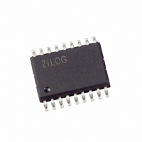
Z8PE003SZ010EG Zilog, Z8PE003SZ010EG Datasheet - Page 15

Z8PE003SZ010EG
Manufacturer Part Number
Z8PE003SZ010EG
Description
IC MICROCONTROLLER 1K 18-SOIC
Manufacturer
Zilog
Series
Z8® Plusr
Specifications of Z8PE003SZ010EG
Core Processor
Z8
Core Size
8-Bit
Speed
10MHz
Peripherals
Brown-out Detect/Reset, POR, PWM, WDT
Number Of I /o
14
Program Memory Size
1KB (1K x 8)
Program Memory Type
OTP
Ram Size
64 x 8
Voltage - Supply (vcc/vdd)
4.5 V ~ 5.5 V
Oscillator Type
Internal
Operating Temperature
-40°C ~ 105°C
Package / Case
18-SOIC (7.5mm Width)
Lead Free Status / RoHS Status
Lead free / RoHS Compliant
Eeprom Size
-
Data Converters
-
Connectivity
-
Other names
269-4294
Z8PE003SZ010EG
Z8PE003SZ010EG
ZiLOG
Z8PLUS CORE
The device is based on the ZiLOG Z8Plus Core Architec-
ture. This core is capable of addressing up to 64KB of pro-
gram memory and 4 KB of RAM. Register RAM is accessed
as either 8- or 16-bit registers using a combination of 4-,
8-, and 12-bit addressing modes. The architecture supports
RESET
This section describes the Z8Plus reset conditions, reset
timing, and register initialization procedures. Reset is gen-
erated by the Voltage Brown-Out/Power-On Reset
(
Recovery (
A system reset overrides all other operating conditions and
puts the Z8Plus device into a known state. To initialize the
chip’s internal logic, the
clock cycles after the oscillator stabilizes. The control reg-
isters and ports are not reset to their default conditions after
wakeup from a
During
The I/O ports and control registers are configured to their
DS007500-Z8X0399
Register (HEX)
FF
FE
FD
FC
FB
FA
F9–F0
EF–E0
DF–D8
D7
D6
D5
Note:
VBO/POR
*The SMR and WDT flags are set to indicate the source of the RESET.
RESET
SMR
), Watch-Dog Timer (
, the value of the program counter is
STOP
).
Register Name
Stack Pointer
Reserved
Register Pointer
Flags
Interrupt Mask
Interrupt
Request
Reserved
Virtual Copy
Reserved
Port B Special
Function
Port B
Directional
Control
Port B Output
mode or
POR
WDT
device counts 64 internal
WDT
time-out.
Table 8. Control and Peripheral Registers*
), and Stop-Mode
U
U
U
7
0
0
0
0
0
U
U
U
6
0
0
0
0
0
P R E L I M I N A R Y
U
U
U
U
5
0
0
0
0
0020H
U
U
U
U
4
0
0
0
0
Bits
.
U
U
U
3
0
0
0
0
0
up to 15 vectored interrupts from external and internal
sources. The processor decodes 44 CISC instructions using
6 addressing modes. See the
information.
default reset state. Resetting the device does not affect the
contents of the general-purpose registers.
The
isters, as shown in Table 8. Specific reset values are indi-
cated by a
or unknown from Power-Up are indicated by the letter
Program execution starts 10 External Crystal (
cycles after the
from location
After a reset, the first routine executed must be one that ini-
tializes the
configuration This activity is followed by initialization of
the remaining control registers.
U
U
U
2
0
0
0
0
0
RESET
U
U
1
0
*
0
0
0
0
1
TCTLHI
circuit initializes the control and peripheral reg-
U Stack pointer is not affected by RESET.
U Output register not affected by RESET.
0
0 Register pointer is not affected by
* Only WDT & SMR flags are affected by
0 All interrupts masked by RESET.
0 All interrupt requests cleared by
0 Deactivates all port special functions
0 Defines all bits as inputs in PortB after
or a
0020H
Comments
RESET.
RESET.
RESET.
Virtual copy of the current working
register set.
after RESET.
RESET.
POR
0
, while bits whose states are unchanged
control register to the required system
. Figure 9 indicates reset timing.
delay. The initial instruction fetch is
Z8Plus User’s Manual
Z8Plus OTP Microcontroller
XTAL
Z8PE003
for more
) clock
U
15
.


