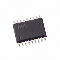
Z8PE003SZ010EG Zilog, Z8PE003SZ010EG Datasheet - Page 34

Z8PE003SZ010EG
Manufacturer Part Number
Z8PE003SZ010EG
Description
IC MICROCONTROLLER 1K 18-SOIC
Manufacturer
Zilog
Series
Z8® Plusr
Specifications of Z8PE003SZ010EG
Core Processor
Z8
Core Size
8-Bit
Speed
10MHz
Peripherals
Brown-out Detect/Reset, POR, PWM, WDT
Number Of I /o
14
Program Memory Size
1KB (1K x 8)
Program Memory Type
OTP
Ram Size
64 x 8
Voltage - Supply (vcc/vdd)
4.5 V ~ 5.5 V
Oscillator Type
Internal
Operating Temperature
-40°C ~ 105°C
Package / Case
18-SOIC (7.5mm Width)
Lead Free Status / RoHS Status
Lead free / RoHS Compliant
Eeprom Size
-
Data Converters
-
Connectivity
-
Other names
269-4294
Z8PE003SZ010EG
Z8PE003SZ010EG
Z8PE003
Z8Plus OTP Microcontroller
for that bit position contains the current synchronized input
value.
For port bits configured as an output by means of the di-
rectional control register, the value held in the correspond-
ing bit of the Output Value Register is driven directly onto
READ/WRITE OPERATIONS
The control for each port is done on a bit-by-bit basis. All
bits are capable of operating as inputs or outputs, depending
on the setting of the port’s directional control register. If
configured as an input, each bit is provided a Schmitt-trig-
ger. The output of the Schmitt-trigger is latched twice to
perform a synchronization function, and the output of the
synchronizer is fed to the port input register, which can be
read by software.
A
dating the contents of the input register, but subsequent
READs
written. If the bit in question is defined as an input, the input
register for that bit position contains the current synchro-
nized input value.
ten on the next clock cycle with the newly sampled input
data. However, if the particular bit is programmed as an out-
put, the input register for that bit retains the software-up-
dated value. The port bits that are programmed as outputs
do not sample the value being driven out.
Any bit in either port can be defined as an output by setting
the appropriate bit in the directional control register. In this
instance, the value held in the appropriate bit of the port out-
put register is driven directly onto the output pin.
Note: The preceding result does not necessarily reflect the actual
PORT A
Port A is a general-purpose port. Figure 27 features a block
diagram of Port A. Each of its lines can be independently
programmed as input or output via the Port A directional
control register (
bit set to a
Port A as an output, while a bit cleared to
corresponding bit in Port A as an input.
The input buffers are Schmitt-triggered. Bits programmed
as outputs can be individually programmed as either push-
34
WRITE
output value. If an external error is holding an output pin ei-
ther High or Low against the output driver, the software
READ
caused by the contention. When a bit is defined as an output,
the Schmitt-trigger on the input is disabled to save power.
do not necessarily return the same value that was
to a port input register carries the effect of up-
1
in
returns the requested value, not the actual state
PTADIR
PTADIR
WRITEs
configures the corresponding bit in
at
to that bit position are overwrit-
0D2H
) as seen in Figure 26. A
0
configures the
P R E L I M I N A R Y
the output pin. The opposite register bit for a given pin (the
output register bit for an input pin and the input register bit
for an output pin) holds their previous value. These bits are
not changed and do not exhibit any effect on the hardware.
Updates to the output register take effect based on the timing
of the internal instruction pipeline; however, this timing is
referenced to the rising edge of the clock. The output reg-
ister can be read at any time, and returns the current output
value that is held. No restrictions are placed on the timing
of
respect to the others.
Note: Care should be taken when updating the directional con-
When updating a directional control register, the special
function register (
caution is not taken, unpredicted events could occur as a re-
sult of the change in the port I/O status. This precaution is
especially important when defining changes in Port B, as
the unpredicted event referred to above could be one or
more interrupts. Clearing of the
first step in configuring the port, while setting the
ister should be the final step in the port configuration pro-
cess. To ensure unpredictable results, the
should not be written until the pins are being driven appro-
priately, and all initialization is completed.
pull or open-drain by setting the corresponding bit in the
special function register (
Register 0D2H
PTADIR Register
D7 D6 D5 D4 D3 D2 D1 D0
READs
Figure 27. Port A Directional Control Register
trol and special function registers.
and/or
WRITEs
SFR
) should first be disabled. If this pre-
PTASFR
to any of the port registers with
1 = Output
0 = Input
SFR
, Figure 26).
register should be the
DS007500-Z8X0399
SFR
SFR
register
ZiLOG
reg-


