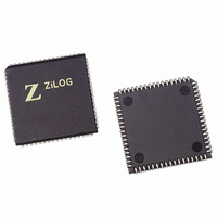
Z86C9620VSC Zilog, Z86C9620VSC Datasheet - Page 21

Z86C9620VSC
Manufacturer Part Number
Z86C9620VSC
Description
IC Z8 20MHZ C91 W/7 PORTS 68PLCC
Manufacturer
Zilog
Series
Z8®r
Datasheet
1.Z86C9620PSC.pdf
(42 pages)
Specifications of Z86C9620VSC
Core Processor
Z8
Core Size
8-Bit
Speed
20MHz
Connectivity
EBI/EMI, UART/USART
Number Of I /o
52
Program Memory Type
ROMless
Ram Size
236 x 8
Voltage - Supply (vcc/vdd)
3 V ~ 5.5 V
Oscillator Type
Internal
Operating Temperature
0°C ~ 70°C
Package / Case
68-PLCC
Lead Free Status / RoHS Status
Contains lead / RoHS non-compliant
Eeprom Size
-
Program Memory Size
-
Data Converters
-
Peripherals
-
Available stocks
Company
Part Number
Manufacturer
Quantity
Price
Company:
Part Number:
Z86C9620VSC
Manufacturer:
ZILOG
Quantity:
5 510
Company:
Part Number:
Z86C9620VSC
Manufacturer:
RURATEL
Quantity:
5 510
Part Number:
Z86C9620VSC
Manufacturer:
ZILOG
Quantity:
20 000
Zilog
Port 1 (P17-P10). Port 1 is an 8-bit, byte programmable,
bidirectional, TTL compatible port. It has multiplexed Ad-
dress (A7-A0) and Data (D7-D0) ports. For Z86C61/62/96,
these eight I/O lines can be programmed as Input or Out-
put lines or can be configured under software control as an
address/data port for interfacing external memory. When
used as an I/O port, Port 1 may be placed under hand-
shake control. In this configuration, Port 3 line P33 and
P34 are used as the handshake controls RDY1 and
/DAV1.
DS97Z8X1600
OEN
Out
In
TTL Level Shifter
MCU
Figure 14. Port 1 Configuration
PS003501-0301
P R E L I M I N A R Y
8
R
500 K
Memory locations greater than 16,384 are referenced
through Port 1. To interface external memory, Port 1 must
be programmed for the multiplexed Address/Data mode. If
more than 256 external locations are required, Port 0 must
output the additional lines.
Port 1 can be placed in high-impedance state along with
Port 0, /AS, /DS, and R//W, allowing the microcontroller to
share common resources in multiprocessor and DMA ap-
plications. Data transfers can be controlled by assigning
P33 as a Bus Acknowledge input, and P34 as a Bus re-
quest output (Figure 14).
Port 1
(AD7-AD0)
Handshake Controls
/DAV1 and RDY1
(P33 and P34)
Auto Latch
CMOS Z8 Microcontroller
PAD
Z86C61/62/96
21
1


