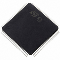
ST10R272LT6 STMicroelectronics, ST10R272LT6 Datasheet - Page 7

ST10R272LT6
Manufacturer Part Number
ST10R272LT6
Description
IC MCU 16BIT LV ROMLESS 100-TQFP
Manufacturer
STMicroelectronics
Series
ST10r
Datasheet
1.ST10R272LT1TR.pdf
(77 pages)
Specifications of ST10R272LT6
Core Processor
ST10
Core Size
16-Bit
Speed
50MHz
Connectivity
EBI/EMI, SSP, UART/USART
Peripherals
POR, PWM, WDT
Number Of I /o
77
Program Memory Type
ROMless
Ram Size
1K x 8
Voltage - Supply (vcc/vdd)
3 V ~ 3.6 V
Oscillator Type
Internal
Operating Temperature
-40°C ~ 85°C
Package / Case
144-TQFP, 144-VQFP
Processor Series
ST10R2x
Core
ST10
Data Bus Width
16 bit
Data Ram Size
1 KB
Interface Type
SSP, USART
Maximum Clock Frequency
50 MHz
Number Of Programmable I/os
77
Number Of Timers
5
Maximum Operating Temperature
+ 85 C
Mounting Style
SMD/SMT
Minimum Operating Temperature
- 40 C
On-chip Adc
16 bit
Lead Free Status / RoHS Status
Contains lead / RoHS non-compliant
Eeprom Size
-
Program Memory Size
-
Data Converters
-
Lead Free Status / Rohs Status
In Transition
Other names
497-2045
Available stocks
Company
Part Number
Manufacturer
Quantity
Price
Company:
Part Number:
ST10R272LT6
Manufacturer:
CYPRESS
Quantity:
1 400
Company:
Part Number:
ST10R272LT6
Manufacturer:
STMicroelectronics
Quantity:
10 000
Part Number:
ST10R272LT6
Manufacturer:
ST
Quantity:
20 000
P4.0–
P4.7
RD
WR/
WRL
READY/
READY
23-26
29-32-
23
...
26
29
30
31
32
33
34
35
I/O
O
...
O
O
O
O
O
O
I/O
O
O
O
O
I
5T
5T
...
5T
5T
5T
5T
5T
5T
5T
5T
5T
5T
5T
5T
Table 1 Pin definitions
An 8-bit bidirectional I/O port. Port 8 is bit-wise programmable
for input or output via direction bits. For a pin configured as
input, the output driver is put into high-impedance state.
Port 4 can be used to output the segment address lines for
external bus configuration.
P4.0
...
P4.3
P4.4
P4.5
P4.6
P4.7
External Memory Read Strobe. RD is activated for every exter-
nal instruction or data read access.
External Memory Write Strobe. In WR-mode, this pin is acti-
vated for every external data write access. In WRL-mode, this
pin is activated for low byte data write accesses on a 16-bit
bus, and for every data write access on an 8-bit bus.
See WRCFG in the SYSCON register for mode selection.
Ready Input. Active level is programmable. When the Ready
function is enabled, the selected inactive level at this pin dur-
ing an external memory access will force the insertion of mem-
ory cycle time waitstates until the pin returns to the selected
active level. Polarity is programmable.
A16
...
A19
A20
SSPCE1
A21
SSPCE0
A22
SSPDAT
A23
SSPCLK
Least Significant Segment Addr. Line
...
Segment Address Line
Segment Address Line
Segment Address Line
SSPChip Enable Line 0
Segment Address Line
SSP Data Input/Output Line
Most Significant Segment Addr. Line
SSP Clock Output Line
Chip Enable Line 1
ST10R272L - PIN DESCRIPTION
7/77
1


