MC9S08SH8CTG Freescale Semiconductor, MC9S08SH8CTG Datasheet - Page 295
MC9S08SH8CTG
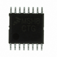
Manufacturer Part Number
MC9S08SH8CTG
Description
IC MCU 8BIT 8K FLASH 16-TSSOP
Manufacturer
Freescale Semiconductor
Series
HCS08r
Datasheet
1.MC9S08SH4CTJ.pdf
(338 pages)
Specifications of MC9S08SH8CTG
Core Processor
HCS08
Core Size
8-Bit
Speed
40MHz
Connectivity
I²C, LIN, SCI, SPI
Peripherals
LVD, POR, PWM, WDT
Number Of I /o
13
Program Memory Size
8KB (8K x 8)
Program Memory Type
FLASH
Ram Size
512 x 8
Voltage - Supply (vcc/vdd)
2.7 V ~ 5.5 V
Data Converters
A/D 8x10b
Oscillator Type
Internal
Operating Temperature
-40°C ~ 85°C
Package / Case
16-TSSOP
Cpu Family
HCS08
Device Core Size
8b
Frequency (max)
40MHz
Interface Type
I2C/SCI/SPI
Total Internal Ram Size
512Byte
# I/os (max)
13
Number Of Timers - General Purpose
1
Operating Supply Voltage (typ)
3.3/5V
Operating Supply Voltage (max)
5.5V
Operating Supply Voltage (min)
2.7V
On-chip Adc
8-chx10-bit
Instruction Set Architecture
CISC
Operating Temp Range
-40C to 85C
Operating Temperature Classification
Industrial
Mounting
Surface Mount
Pin Count
16
Package Type
TSSOP
Processor Series
S08SH
Core
HCS08
Data Bus Width
8 bit
Data Ram Size
512 B
Maximum Clock Frequency
40 MHz
Number Of Programmable I/os
13
Number Of Timers
3
Operating Supply Voltage
5.5 V
Maximum Operating Temperature
+ 85 C
Mounting Style
SMD/SMT
3rd Party Development Tools
EWS08
Development Tools By Supplier
DEMO9S08SG32, DEMO9S08SG32AUTO, DEMO9S08SG8, DEMO9S08SG8AUTO, DEMO9S08SH32, DEMO9S08SH8
Minimum Operating Temperature
- 40 C
For Use With
DEMO9S08SH8 - BOARD DEMO FOR MC9S08SH FAM
Lead Free Status / RoHS Status
Lead free / RoHS Compliant
Eeprom Size
-
Lead Free Status / Rohs Status
Compliant
Available stocks
Company
Part Number
Manufacturer
Quantity
Price
Company:

Part Number:
MC9S08SH8CTG
Manufacturer:
FREESCALE
Quantity:
12 000
Part Number:
MC9S08SH8CTG
Manufacturer:
FREESCALE
Quantity:
20 000
Part Number:
MC9S08SH8CTGR
Manufacturer:
FREESCALE
Quantity:
20 000


1
2
3
4
5
6
7
8
9
10
Num C
Freescale Semiconductor
15
16
17
18
19
20
21
22
23
24
Typical values are measured at 25°C. Characterized, not tested.
When IRQ or a pin interrupt is configured to detect rising edges, pulldown resistors are used in place of pullup resistors.
The specified resistor value is the actual value internal to the device. The pullup value may measure higher when measured
externally on the pin.
Power supply must maintain regulation within operating V
conditions. If positive injection current (V
in external power supply going out of regulation. Ensure external V
current. This will be the greatest risk when the MCU is not consuming power. Examples are: if no system clock is present, or if
clock rate is very low (which would reduce overall power consumption).
All functional non-supply pins are internally clamped to V
Input must be current limited to the value specified. To determine the value of the required current-limiting resistor, calculate
resistance values for positive and negative clamp voltages, then use the larger of the two values.
The RESET pin does not have a clamp diode to V
Maximum is highest voltage that POR will occur.
Simulated, not tested
Factory trimmed at V
D POR re-arm voltage
D POR re-arm time
P Low-voltage detection threshold —
P
P
P
P
P
P Bandgap Voltage Reference
T Low-voltage inhibit reset/recover
high range
Low-voltage detection threshold —
low range
Low-voltage warning threshold —
high range 1
Low-voltage warning threshold —
high range 0
Low-voltage warning threshold
low range 1
Low-voltage warning threshold —
low range 0
hysteresis
DD
Characteristic
= 5.0 V, Temp = 25°C
9
8
Table A-6. DC Characteristics (continued)
10
V
V
V
V
V
V
MC9S08SH8 MCU Series Data Sheet, Rev. 3
V
V
V
V
V
V
DD
DD
DD
DD
DD
DD
In
DD
DD
DD
DD
DD
DD
> V
falling
falling
falling
falling
falling
falling
rising
rising
rising
rising
rising
rising
DD
) is greater than I
DD
Symbol
V
V
V
V
V
V
. Do not drive this pin above V
V
t
V
V
POR
LVW3
LVW2
LVW1
LVW0
LVD1
LVD0
POR
hys
BG
SS
DD
and V
range during instantaneous and operating maximum current
DD
DD
DD
Condition
, the injection current may flow out of V
.
load will shunt current greater than maximum injection
5 V
3 V
.
DD
.
2.48
2.54
2.84
2.90
2.66
2.72
1.18
Min
0.9
3.9
4.0
4.5
4.6
4.2
4.3
10
—
—
Appendix A Electrical Characteristics
Typ
2.56
2.62
2.92
2.98
2.74
2.80
1.20
100
1.4
4.0
4.1
4.6
4.7
4.3
4.4
60
—
1
DD
and could result
Max
2.64
2.70
3.00
3.06
2.82
2.88
1.21
2.0
4.1
4.2
4.7
4.8
4.4
4.5
—
—
—
Unit
mV
μs
V
V
V
V
V
V
V
V
295
Related parts for MC9S08SH8CTG
Image
Part Number
Description
Manufacturer
Datasheet
Request
R

Part Number:
Description:
Manufacturer:
Freescale Semiconductor, Inc
Datasheet:
Part Number:
Description:
Manufacturer:
Freescale Semiconductor, Inc
Datasheet:
Part Number:
Description:
Manufacturer:
Freescale Semiconductor, Inc
Datasheet:
Part Number:
Description:
Manufacturer:
Freescale Semiconductor, Inc
Datasheet:
Part Number:
Description:
Manufacturer:
Freescale Semiconductor, Inc
Datasheet:
Part Number:
Description:
Manufacturer:
Freescale Semiconductor, Inc
Datasheet:
Part Number:
Description:
Manufacturer:
Freescale Semiconductor, Inc
Datasheet:
Part Number:
Description:
Manufacturer:
Freescale Semiconductor, Inc
Datasheet:
Part Number:
Description:
Manufacturer:
Freescale Semiconductor, Inc
Datasheet:
Part Number:
Description:
Manufacturer:
Freescale Semiconductor, Inc
Datasheet:
Part Number:
Description:
Manufacturer:
Freescale Semiconductor, Inc
Datasheet:
Part Number:
Description:
Manufacturer:
Freescale Semiconductor, Inc
Datasheet:
Part Number:
Description:
Manufacturer:
Freescale Semiconductor, Inc
Datasheet:
Part Number:
Description:
Manufacturer:
Freescale Semiconductor, Inc
Datasheet:
Part Number:
Description:
Manufacturer:
Freescale Semiconductor, Inc
Datasheet: