C8051F521A-IM Silicon Laboratories Inc, C8051F521A-IM Datasheet - Page 113
C8051F521A-IM
Manufacturer Part Number
C8051F521A-IM
Description
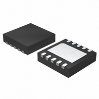
IC 8051 MCU 8K FLASH 10DFN
Manufacturer
Silicon Laboratories Inc
Series
C8051F52xr
Specifications of C8051F521A-IM
Program Memory Type
FLASH
Program Memory Size
8KB (8K x 8)
Package / Case
10-DFN
Core Processor
8051
Core Size
8-Bit
Speed
25MHz
Connectivity
SPI, UART/USART
Peripherals
Brown-out Detect/Reset, POR, PWM, Temp Sensor, WDT
Number Of I /o
6
Ram Size
256 x 8
Voltage - Supply (vcc/vdd)
1.8 V ~ 5.25 V
Data Converters
A/D 6x12b
Oscillator Type
Internal
Operating Temperature
-40°C ~ 125°C
Processor Series
C8051F5x
Core
8051
Data Bus Width
8 bit
Data Ram Size
256 B
Interface Type
SPI/UART
Maximum Clock Frequency
25 MHz
Number Of Programmable I/os
6
Number Of Timers
3
Maximum Operating Temperature
+ 125 C
Mounting Style
SMD/SMT
3rd Party Development Tools
PK51, CA51, A51, ULINK2
Development Tools By Supplier
C8051F500DK
Minimum Operating Temperature
- 40 C
On-chip Adc
6-ch x 12-bit
Lead Free Status / RoHS Status
Lead free / RoHS Compliant
For Use With
336-1488 - KIT DEV C8051F53XA, C8051F52XA770-1006 - ISP 4PORT FOR SILABS C8051F MCU336-1455 - ADAPTER PROGRAM TOOLSTICK F520
Eeprom Size
-
Lead Free Status / Rohs Status
Lead free / RoHS Compliant
Other names
336-1490-5


C8051F52x/F52xA/F53x/F53xA
12.1.2. Flash Erase Procedure
The Flash memory can be programmed by software using the MOVX write instruction with the address and
data byte to be programmed provided as normal operands. Before writing to Flash memory using MOVX,
Flash write operations must be enabled by: (1) setting the PSWE Program Store Write Enable bit
(PSCTL.0) to logic 1 (this directs the MOVX writes to target Flash memory); and (2) Writing the Flash key
codes in sequence to the Flash Lock register (FLKEY). The PSWE bit remains set until cleared by soft-
ware.
A write to Flash memory can clear bits to logic 0 but cannot set them; only an erase operation can set bits
to logic 1 in Flash. A byte location to be programmed should be erased before a new value is written.
The Flash memory is organized in 512-byte pages. The erase operation applies to an entire page (setting
all bytes in the page to 0xFF). To erase an entire 512-byte page, perform the following steps:
1. Disable interrupts (recommended).
2. Write the first key code to FLKEY: 0xA5.
3. Write the second key code to FLKEY: 0xF1.
4. Set the PSEE bit (register PSCTL).
5. Set the PSWE bit (register PSCTL).
6. Using the MOVX instruction, write a data byte to any location within the 512-byte page to be erased.
7. Clear the PSWE and PSEE bits.
8. Re-enable interrupts.
12.1.3. Flash Write Procedure
Flash bytes are programmed by software with the following sequence:
1. Disable interrupts.
2. Write the first key code to FLKEY: 0xA5.
3. Write the second key code to FLKEY: 0xF1.
4. Set the PSWE bit (register PSCTL).
5. Clear the PSEE bit (register PSCTL).
6. Using the MOVX instruction, write a single data byte to the desired location within the 512-byte sector.
7. Clear the PSWE bit.
8. Re-enable interrupts.
Steps 2–7 must be repeated for each byte to be written. After Flash writes are complete, PSWE should be
cleared so that MOVX instructions do not target program memory.
Rev. 1.3
113
Related parts for C8051F521A-IM
Image
Part Number
Description
Manufacturer
Datasheet
Request
R

Part Number:
Description:
SMD/C°/SINGLE-ENDED OUTPUT SILICON OSCILLATOR
Manufacturer:
Silicon Laboratories Inc
Part Number:
Description:
Manufacturer:
Silicon Laboratories Inc
Datasheet:
Part Number:
Description:
N/A N/A/SI4010 AES KEYFOB DEMO WITH LCD RX
Manufacturer:
Silicon Laboratories Inc
Datasheet:
Part Number:
Description:
N/A N/A/SI4010 SIMPLIFIED KEY FOB DEMO WITH LED RX
Manufacturer:
Silicon Laboratories Inc
Datasheet:
Part Number:
Description:
N/A/-40 TO 85 OC/EZLINK MODULE; F930/4432 HIGH BAND (REV E/B1)
Manufacturer:
Silicon Laboratories Inc
Part Number:
Description:
EZLink Module; F930/4432 Low Band (rev e/B1)
Manufacturer:
Silicon Laboratories Inc
Part Number:
Description:
I°/4460 10 DBM RADIO TEST CARD 434 MHZ
Manufacturer:
Silicon Laboratories Inc
Part Number:
Description:
I°/4461 14 DBM RADIO TEST CARD 868 MHZ
Manufacturer:
Silicon Laboratories Inc
Part Number:
Description:
I°/4463 20 DBM RFSWITCH RADIO TEST CARD 460 MHZ
Manufacturer:
Silicon Laboratories Inc
Part Number:
Description:
I°/4463 20 DBM RADIO TEST CARD 868 MHZ
Manufacturer:
Silicon Laboratories Inc
Part Number:
Description:
I°/4463 27 DBM RADIO TEST CARD 868 MHZ
Manufacturer:
Silicon Laboratories Inc
Part Number:
Description:
I°/4463 SKYWORKS 30 DBM RADIO TEST CARD 915 MHZ
Manufacturer:
Silicon Laboratories Inc
Part Number:
Description:
N/A N/A/-40 TO 85 OC/4463 RFMD 30 DBM RADIO TEST CARD 915 MHZ
Manufacturer:
Silicon Laboratories Inc
Part Number:
Description:
I°/4463 20 DBM RADIO TEST CARD 169 MHZ
Manufacturer:
Silicon Laboratories Inc