C8051F521A-IM Silicon Laboratories Inc, C8051F521A-IM Datasheet - Page 8
C8051F521A-IM
Manufacturer Part Number
C8051F521A-IM
Description
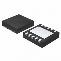
IC 8051 MCU 8K FLASH 10DFN
Manufacturer
Silicon Laboratories Inc
Series
C8051F52xr
Specifications of C8051F521A-IM
Program Memory Type
FLASH
Program Memory Size
8KB (8K x 8)
Package / Case
10-DFN
Core Processor
8051
Core Size
8-Bit
Speed
25MHz
Connectivity
SPI, UART/USART
Peripherals
Brown-out Detect/Reset, POR, PWM, Temp Sensor, WDT
Number Of I /o
6
Ram Size
256 x 8
Voltage - Supply (vcc/vdd)
1.8 V ~ 5.25 V
Data Converters
A/D 6x12b
Oscillator Type
Internal
Operating Temperature
-40°C ~ 125°C
Processor Series
C8051F5x
Core
8051
Data Bus Width
8 bit
Data Ram Size
256 B
Interface Type
SPI/UART
Maximum Clock Frequency
25 MHz
Number Of Programmable I/os
6
Number Of Timers
3
Maximum Operating Temperature
+ 125 C
Mounting Style
SMD/SMT
3rd Party Development Tools
PK51, CA51, A51, ULINK2
Development Tools By Supplier
C8051F500DK
Minimum Operating Temperature
- 40 C
On-chip Adc
6-ch x 12-bit
Lead Free Status / RoHS Status
Lead free / RoHS Compliant
For Use With
336-1488 - KIT DEV C8051F53XA, C8051F52XA770-1006 - ISP 4PORT FOR SILABS C8051F MCU336-1455 - ADAPTER PROGRAM TOOLSTICK F520
Eeprom Size
-
Lead Free Status / Rohs Status
Lead free / RoHS Compliant
Other names
336-1490-5


C8051F52x/F52xA/F53x/F53xA
8
Figure 14.2. 32 kHz External Crystal Example ...................................................... 139
Figure 15.1. UART0 Block Diagram ...................................................................... 143
Figure 15.2. UART0 Baud Rate Logic ................................................................... 144
Figure 15.3. UART Interconnect Diagram ............................................................. 145
Figure 15.4. 8-Bit UART Timing Diagram .............................................................. 145
Figure 15.5. 9-Bit UART Timing Diagram .............................................................. 146
Figure 15.6. UART Multi-Processor Mode Interconnect Diagram ......................... 147
Figure 16.1. SPI Block Diagram ............................................................................ 150
Figure 16.2. Multiple-Master Mode Connection Diagram ...................................... 153
Figure 16.3. 3-Wire Single Master and Slave Mode Connection Diagram ............ 153
Figure 16.4. 4-Wire Single Master and Slave Mode Connection Diagram ............ 153
Figure 16.5. Data/Clock Timing Relationship ........................................................ 155
Figure 16.6. SPI Master Timing (CKPHA = 0) ....................................................... 160
Figure 16.7. SPI Master Timing (CKPHA = 1) ....................................................... 160
Figure 16.8. SPI Slave Timing (CKPHA = 0) ......................................................... 161
Figure 16.9. SPI Slave Timing (CKPHA = 1) ......................................................... 161
Figure 17.1. LIN Block Diagram ............................................................................ 163
Figure 18.1. T0 Mode 0 Block Diagram ................................................................. 182
Figure 18.2. T0 Mode 2 Block Diagram ................................................................. 183
Figure 18.3. T0 Mode 3 Block Diagram ................................................................. 184
Figure 18.4. Timer 2 16-Bit Mode Block Diagram ................................................. 189
Figure 18.5. Timer 2 8-Bit Mode Block Diagram ................................................... 190
Figure 18.6. Timer 2 Capture Mode Block Diagram .............................................. 191
Figure 19.1. PCA Block Diagram ........................................................................... 194
Figure 19.2. PCA Counter/Timer Block Diagram ................................................... 195
Figure 19.3. PCA Interrupt Block Diagram ............................................................ 196
Figure 19.4. PCA Capture Mode Diagram ............................................................. 197
Figure 19.5. PCA Software Timer Mode Diagram ................................................. 198
Figure 19.6. PCA High-Speed Output Mode Diagram ........................................... 199
Figure 19.7. PCA Frequency Output Mode ........................................................... 200
Figure 19.8. PCA 8-Bit PWM Mode Diagram ........................................................ 201
Figure 19.9. PCA 16-Bit PWM Mode ..................................................................... 202
Figure 19.10. PCA Module 2 with Watchdog Timer Enabled ................................ 203
Figure 20.1. Device Package—TSSOP 20 ............................................................ 209
Figure 20.2. Device Package—QFN 20 ................................................................ 209
Figure 20.3. Device Package—DFN 10 ................................................................ 210
Figure 21.1. Typical C2 Pin Sharing ...................................................................... 214
Rev. 1.3
Related parts for C8051F521A-IM
Image
Part Number
Description
Manufacturer
Datasheet
Request
R

Part Number:
Description:
SMD/C°/SINGLE-ENDED OUTPUT SILICON OSCILLATOR
Manufacturer:
Silicon Laboratories Inc
Part Number:
Description:
Manufacturer:
Silicon Laboratories Inc
Datasheet:
Part Number:
Description:
N/A N/A/SI4010 AES KEYFOB DEMO WITH LCD RX
Manufacturer:
Silicon Laboratories Inc
Datasheet:
Part Number:
Description:
N/A N/A/SI4010 SIMPLIFIED KEY FOB DEMO WITH LED RX
Manufacturer:
Silicon Laboratories Inc
Datasheet:
Part Number:
Description:
N/A/-40 TO 85 OC/EZLINK MODULE; F930/4432 HIGH BAND (REV E/B1)
Manufacturer:
Silicon Laboratories Inc
Part Number:
Description:
EZLink Module; F930/4432 Low Band (rev e/B1)
Manufacturer:
Silicon Laboratories Inc
Part Number:
Description:
I°/4460 10 DBM RADIO TEST CARD 434 MHZ
Manufacturer:
Silicon Laboratories Inc
Part Number:
Description:
I°/4461 14 DBM RADIO TEST CARD 868 MHZ
Manufacturer:
Silicon Laboratories Inc
Part Number:
Description:
I°/4463 20 DBM RFSWITCH RADIO TEST CARD 460 MHZ
Manufacturer:
Silicon Laboratories Inc
Part Number:
Description:
I°/4463 20 DBM RADIO TEST CARD 868 MHZ
Manufacturer:
Silicon Laboratories Inc
Part Number:
Description:
I°/4463 27 DBM RADIO TEST CARD 868 MHZ
Manufacturer:
Silicon Laboratories Inc
Part Number:
Description:
I°/4463 SKYWORKS 30 DBM RADIO TEST CARD 915 MHZ
Manufacturer:
Silicon Laboratories Inc
Part Number:
Description:
N/A N/A/-40 TO 85 OC/4463 RFMD 30 DBM RADIO TEST CARD 915 MHZ
Manufacturer:
Silicon Laboratories Inc
Part Number:
Description:
I°/4463 20 DBM RADIO TEST CARD 169 MHZ
Manufacturer:
Silicon Laboratories Inc