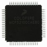
MCF52100CAE80 Freescale Semiconductor, MCF52100CAE80 Datasheet - Page 19

MCF52100CAE80
Manufacturer Part Number
MCF52100CAE80
Description
IC MCU 32BIT 80MHZ 64-LQFP
Manufacturer
Freescale Semiconductor
Series
MCF521xxr
Datasheet
1.MCF52110CAF80.pdf
(56 pages)
Specifications of MCF52100CAE80
Core Processor
Coldfire V2
Core Size
32-Bit
Speed
80MHz
Connectivity
I²C, SPI, UART/USART
Peripherals
DMA, LVD, POR, PWM, WDT
Number Of I /o
43
Program Memory Size
64KB (64K x 8)
Program Memory Type
FLASH
Ram Size
16K x 8
Voltage - Supply (vcc/vdd)
3 V ~ 3.6 V
Data Converters
A/D 8x12b
Oscillator Type
Internal
Operating Temperature
-40°C ~ 85°C
Package / Case
64-LQFP
Processor Series
MCF521x
Core
ColdFire V2
Data Bus Width
32 bit
Data Ram Size
16 KB
Interface Type
I2C/QSPI/UART
Maximum Clock Frequency
80 MHz
Number Of Programmable I/os
56
Number Of Timers
10
Operating Supply Voltage
- 0.3 V to + 4 V
Maximum Operating Temperature
+ 85 C
Mounting Style
SMD/SMT
3rd Party Development Tools
JLINK-CF-BDM26, EWCF
Development Tools By Supplier
M52210DEMO
Minimum Operating Temperature
- 40 C
On-chip Adc
8-ch x 12-bit
For Use With
M5211DEMO - KIT DEMO FOR MCF5211
Lead Free Status / RoHS Status
Lead free / RoHS Compliant
Eeprom Size
-
Lead Free Status / Rohs Status
Lead free / RoHS Compliant
1
2
3
4
5
6
7
8
9
The PDSR and PSSR registers are described in the General Purpose I/O chapter. All programmable signals default to 2 mA drive and FAST slew rate in
All signals have a pull-up in GPIO mode.
These signals are multiplexed on other pins.
For primary and GPIO functions only.
Only when JTAG mode is enabled.
CLKMOD0 and CLKMOD1 have internal pull-down resistors; however, the use of external resistors is very strongly recommended.
For secondary and GPIO functions only.
RSTI has an internal pull-up resistor; however, the use of an external resistor is very strongly recommended.
For GPIO function. Primary Function has pull-up control within the GPT module.
normal (single-chip) mode.
UART 1
UART 2
VSTBY
Group
VDD
VSS
Pin
Function
Primary
UCTS1
URXD1
UTXD1
UCTS2
URXD2
UTXD2
VSTBY
URTS1
URTS2
VDD
VSS
Secondary
Function
SYNCA
SYNCB
SDA1
SCL1
SCL1
SDA1
—
—
—
—
—
Table 3. Pin Functions by Primary and Alternate Purpose (continued)
Function
Tertiary
URXD2
UTXD2
—
—
—
—
—
—
—
—
—
Quaternary
Function
GPIO
GPIO
GPIO
GPIO
GPIO
GPIO
GPIO
GPIO
—
—
—
Strength /
PDSR[15]
PDSR[14]
PDSR[13]
PDSR[12]
PDSR[27]
PDSR[26]
PDSR[25]
PDSR[24]
Control
Drive
N/A
N/A
N/A
1
Slew Rate /
PSRR[15]
PSRR[14]
PSRR[13]
PSRR[12]
PSRR[27]
PSRR[26]
PSRR[25]
PSRR[24]
Control
N/A
N/A
N/A
1
Pull-down
Pull-up /
—
—
—
—
—
—
—
—
—
—
—
2
3,15,24,25,3
57,68,81,93
67,75,82,92
100 LQFP
1,2,14,22,
23,34,41,
5,42,56,
Pin on
100
98
99
27
30
28
29
55
4
A1,A9,D4,D
D5,E3–E7,
6,F4,F6,J1
Pin on 81
MAPBGA
C3
B1
B2
A2
F8
F5
—
—
—
—
1,10,20,39,5
LQFP/QFN
Pin on 64
11,21,38,
53,64
61
63
62
—
—
—
—
37
2
2


