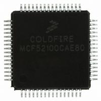
MCF52100CAE80 Freescale Semiconductor, MCF52100CAE80 Datasheet - Page 20
MCF52100CAE80
Manufacturer Part Number
MCF52100CAE80
Description
IC MCU 32BIT 80MHZ 64-LQFP
Manufacturer
Freescale Semiconductor
Series
MCF521xxr
Datasheet
1.MCF52110CAF80.pdf
(56 pages)
Specifications of MCF52100CAE80
Core Processor
Coldfire V2
Core Size
32-Bit
Speed
80MHz
Connectivity
I²C, SPI, UART/USART
Peripherals
DMA, LVD, POR, PWM, WDT
Number Of I /o
43
Program Memory Size
64KB (64K x 8)
Program Memory Type
FLASH
Ram Size
16K x 8
Voltage - Supply (vcc/vdd)
3 V ~ 3.6 V
Data Converters
A/D 8x12b
Oscillator Type
Internal
Operating Temperature
-40°C ~ 85°C
Package / Case
64-LQFP
Processor Series
MCF521x
Core
ColdFire V2
Data Bus Width
32 bit
Data Ram Size
16 KB
Interface Type
I2C/QSPI/UART
Maximum Clock Frequency
80 MHz
Number Of Programmable I/os
56
Number Of Timers
10
Operating Supply Voltage
- 0.3 V to + 4 V
Maximum Operating Temperature
+ 85 C
Mounting Style
SMD/SMT
3rd Party Development Tools
JLINK-CF-BDM26, EWCF
Development Tools By Supplier
M52210DEMO
Minimum Operating Temperature
- 40 C
On-chip Adc
8-ch x 12-bit
For Use With
M5211DEMO - KIT DEMO FOR MCF5211
Lead Free Status / RoHS Status
Lead free / RoHS Compliant
Eeprom Size
-
Lead Free Status / Rohs Status
Lead free / RoHS Compliant


Family Configurations
1.3
Table 4
1.4
Table 5
1.5
Table 6
20
Clock Mode Selection
Reset Configuration
describes signals used to reset the chip or as a reset indication.
describes signals used to support the on-chip clock generation circuitry.
describes signals used in mode selection;
External Clock In
Signal Name
Signal Name
Signal Name
Reset Out
Reset Signals
PLL and Clock Signals
Mode Selection
Clock Out
Reset In
Crystal
Test
CLKMOD[1:0]
00
00
01
10
10
11
Abbreviation
Abbreviation
CLKMOD[1:0] Selects the clock boot mode.
Abbreviation
CLKOUT
RSTO
EXTAL
RSTI
XTAL
RCON
XTAL
TEST
N/A
N/A
0
1
0
1
MCF52110 ColdFire Microcontroller, Rev. 1
Table 6. Mode Selection Signals
Primary reset input to the device. Asserting RSTI for at least 8 CPU
clock cycles immediately resets the CPU and peripherals.
Driven low for 1024 CPU clocks after the reset source has deasserted.
Table 5. PLL and Clock Signals
PLL disabled, clock driven by external oscillator
PLL disabled, clock driven by on-chip oscillator
PLL disabled, clock driven by crystal
PLL in normal mode, clock driven by external oscillator
Reserved
PLL in normal mode, clock driven by crystal
Crystal oscillator or external clock input except when the on-chip
relaxation oscillator is used.
Crystal oscillator output except when CLKMOD0=0, then sampled as
part of the clock mode selection mechanism.
This output signal reflects the internal system clock.
The Serial Flash Programming mode is entered by asserting the
RCON pin (with the TEST pin negated) as the chip comes out of
reset. During this mode, the EzPort has access to the flash memory
which can be programmed from an external device.
Reserved for factory testing only and in normal modes of operation
should be connected to VSS to prevent unintentional activation of
test functions.
Table 7. Clocking Modes
Table 7
Table 4. Reset Signals
2
describes the particular clocking modes.
Configure the clock mode.
Function
Function
Function
1
Freescale Semiconductor
I/O
I/O
I/O
O
O
O
I
I
I
I
Related parts for MCF52100CAE80
Image
Part Number
Description
Manufacturer
Datasheet
Request
R

Part Number:
Description:
Manufacturer:
Freescale Semiconductor, Inc
Datasheet:
Part Number:
Description:
Manufacturer:
Freescale Semiconductor, Inc
Datasheet:
Part Number:
Description:
Manufacturer:
Freescale Semiconductor, Inc
Datasheet:
Part Number:
Description:
Manufacturer:
Freescale Semiconductor, Inc
Datasheet:
Part Number:
Description:
Manufacturer:
Freescale Semiconductor, Inc
Datasheet:
Part Number:
Description:
Manufacturer:
Freescale Semiconductor, Inc
Datasheet:
Part Number:
Description:
Manufacturer:
Freescale Semiconductor, Inc
Datasheet:
Part Number:
Description:
Manufacturer:
Freescale Semiconductor, Inc
Datasheet:
Part Number:
Description:
Manufacturer:
Freescale Semiconductor, Inc
Datasheet:
Part Number:
Description:
Manufacturer:
Freescale Semiconductor, Inc
Datasheet:
Part Number:
Description:
Manufacturer:
Freescale Semiconductor, Inc
Datasheet:
Part Number:
Description:
Manufacturer:
Freescale Semiconductor, Inc
Datasheet:
Part Number:
Description:
Manufacturer:
Freescale Semiconductor, Inc
Datasheet:
Part Number:
Description:
Manufacturer:
Freescale Semiconductor, Inc
Datasheet:
Part Number:
Description:
Manufacturer:
Freescale Semiconductor, Inc
Datasheet: